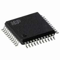
SAA7129H/V1,518 NXP Semiconductors, SAA7129H/V1,518 Datasheet - Page 13

SAA7129H/V1,518
Manufacturer Part Number
SAA7129H/V1,518
Description
IC DIGITAL VIDEO DECODER 44QFP
Manufacturer
NXP Semiconductors
Type
Video Encoderr
Datasheet
1.SAA7129HV1557.pdf
(55 pages)
Specifications of SAA7129H/V1,518
Voltage - Supply, Analog
3.1 V ~ 3.5 V
Voltage - Supply, Digital
3 V ~ 3.6 V
Mounting Type
Surface Mount
Package / Case
44-MQFP, 44-PQFP
Lead Free Status / RoHS Status
Lead free / RoHS Compliant
Applications
-
Other names
935262601518
SAA7129HB-T
SAA7129HB-T
SAA7129HB-T
SAA7129HB-T
Available stocks
Company
Part Number
Manufacturer
Quantity
Price
Company:
Part Number:
SAA7129H/V1,518
Manufacturer:
NXP Semiconductors
Quantity:
10 000
Philips Semiconductors
9397 750 14325
Product data sheet
7.8 Clock
7.9 I
The horizontal phase can be set via a separate input RCV2. In the event of VS pulses at
RCV1, this is mandatory. It is also possible to set the signal path to blank via this input.
From the ITU-R BT.656 data stream, the SAA7128H; SAA7129H decodes only the start of
the first line in the odd field. All other information is ignored and may miss. If this kind of
slave mode is active, the RCV pins may be switched to output mode.
In slave mode, the horizontal trigger phase can be programmed to any point in the line,
the vertical phase from line 0 to line 15 counted from the first serration pulse in half line
steps.
Whenever synchronization information cannot be derived directly from the inputs, the
SAA7128H; SAA7129H will calculate it from the internal horizontal, vertical and PAL
phase. This gives good flexibility with respect to external synchronization, but the circuit
does not suppress illegal settings. In such an event, the odd/even information may vanish
as it does in the non-interlaced modes.
In master mode, the line lengths are fixed to 1728 clocks at 50 Hz and 1716 clocks at
60 Hz. To allow non-interlaced frames, the field lengths can be varied by 0.5 lines. In the
event of non-interlace, the SAA7128H; SAA7129H does not provide odd/even information
and the output signal does not contain the PAL ‘Bruch sequence’.
At the RCV1 pin the IC can provide:
At the RCV2 pin, there is a horizontal pulse of programmable phase and duration
available. This pulse can be suppressed in the programmable inactive part of a field,
giving a composite blank signal.
The directions and polarities of the RCV ports can be chosen independently. Timing
references can be found in
The input to LLC1 can either be an external clock source or the buffered on-chip clock
XCLK. The internal crystal oscillator can be run with either a 3rd-harmonic or a
fundamental crystal frequency.
The I
and 400 kbit/s guaranteed transfer rate. It uses 8-bit subaddressing with an
auto-increment function. All registers are write and readable, except one read only status
byte.
The I
pin 21 (SA) tied HIGH.
2
•
•
•
C-bus interface
A Vertical Sync (VS) signal with 2.5 (50 Hz) or 3 (60 Hz) lines duration
An odd/even signal which is LOW in odd fields
A Field Sequence (FSEQ) signal which is HIGH in the first field of the 4 or 8 or 12 field
sequences.
2
2
C-bus interface is a standard slave transceiver, supporting 7-bit slave addresses
C-bus slave address is defined as 88h with pin 21 (SA) tied LOW and as 8Ch with
Rev. 03 — 9 December 2004
Table 55
and
SAA7128H; SAA7129H
Table
63.
© Koninklijke Philips Electronics N.V. 2004. All rights reserved.
Digital video encoder
13 of 55


