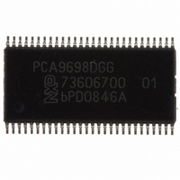
PCA9698DGG,512 NXP Semiconductors, PCA9698DGG,512 Datasheet - Page 28

PCA9698DGG,512
Manufacturer Part Number
PCA9698DGG,512
Description
IC I/O EXPANDER I2C 40B 56TSSOP
Manufacturer
NXP Semiconductors
Datasheet
1.PCA9698BS118.pdf
(48 pages)
Specifications of PCA9698DGG,512
Package / Case
56-TSSOP
Interface
I²C
Number Of I /o
40
Interrupt Output
Yes
Frequency - Clock
1MHz
Voltage - Supply
2.3 V ~ 5.5 V
Operating Temperature
-40°C ~ 85°C
Mounting Type
Surface Mount
Includes
POR
Logic Family
PCA9698
Number Of Lines (input / Output)
40.0 / 40.0
Operating Supply Voltage
2.3 V to 5.5 V
Power Dissipation
500 mW
Operating Temperature Range
- 40 C to + 85 C
Input Voltage
5.5 V
Logic Type
I2C Bus
Maximum Clock Frequency
1 MHz
Mounting Style
SMD/SMT
Number Of Input Lines
40.0
Number Of Output Lines
40.0
Output Current
50 mA
Output Voltage
5.5 V
Lead Free Status / RoHS Status
Lead free / RoHS Compliant
For Use With
OM6281 - DAUGHTER CARD PCA9698 FOR OM6275
Lead Free Status / Rohs Status
Lead free / RoHS Compliant
Other names
568-3241-5
935278614512
PCA9698DGG
935278614512
PCA9698DGG
Available stocks
Company
Part Number
Manufacturer
Quantity
Price
Part Number:
PCA9698DGG,512
Manufacturer:
NXP/恩智浦
Quantity:
20 000
NXP Semiconductors
PCA9698
Product data sheet
Fig 18. Write to the output structure configuration, all bank control, or mode selection
Fig 19. Read from Input Port, Output Port, I/O Configuration, Polarity Inversion, or Mask interrupt registers
The programming becomes effective at the Acknowledge.
If more than 1 byte is written, previous data is overwritten.
If AI = 0, the same register is read during the whole sequence.
If AI = 1, the register value is incremented after each read. When the last register bank is read, it rolls over to the first byte of the
category (see category definition in
The INT signal is released only when the last register containing an input that changed has been read. For example, when
IO2_4 and IO4_7 change at the same time and an Input Port register read sequence is initiated, starting with IP0, INT is
released after IP4 is read (and not after IP2 is read).
SDA
SDA
S A6 A5 A4 A3 A2 A1 A0 0 A
START condition
S A6 A5 A4 A3 A2 A1 A0 0 A
START condition
register determined
by D4 D3 D2 D1 D0
data from register
slave address
first byte
slave address
DATA
acknowledge
acknowledge
from slave
from slave
R/W
A
acknowledge
from master
R/W
Section 7.3 “Command
All information provided in this document is subject to legal disclaimers.
data from register
AI = 1
1
second byte
AI = 'don't care'
X
0 D5 D4 D3 D2 D1 D0
DATA
command register
40-bit Fm+ I
0
Rev. 3 — 3 August 2010
command register
1
0
1
acknowledge
D[5:0] = 00 0000 for Input Port register bank 0
D[5:0] = 00 1000 for Output Port register bank 0
D[5:0] = 01 0000 for Polarity Inversion register bank 0
D[5:0] = 01 1000 for Configuration register bank 0
D[5:0] = 10 0000 for Mask Interrupt register bank 0
from slave
0 D1 D0
register”).
2
C-bus advanced I/O port with RESET, OE and INT
A
A
Sr
acknowledge
from slave
00 for output structure configuration programming
01 for all bank control register programming
10 for mode selection register programming
repeated START
condition
A6 A5 A4 A3 A2 A1 A0
DATA
slave address
data from register
last byte
DATA
A
acknowledge
from slave
P
STOP condition
acknowledge
from slave
R/W
1 A
A
no acknowledge
from master
P
STOP condition
PCA9698
002aab947
© NXP B.V. 2010. All rights reserved.
002aab948
28 of 48


