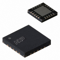
PCA9501BS,118 NXP Semiconductors, PCA9501BS,118 Datasheet - Page 9

PCA9501BS,118
Manufacturer Part Number
PCA9501BS,118
Description
IC I/O EXPANDER I2C 8B 20HVQFN
Manufacturer
NXP Semiconductors
Datasheet
1.PCA9501BS118.pdf
(28 pages)
Specifications of PCA9501BS,118
Package / Case
20-VQFN Exposed Pad, 20-HVQFN, 20-SQFN, 20-DHVQFN
Interface
I²C, SMBus
Number Of I /o
8
Interrupt Output
Yes
Frequency - Clock
400kHz
Voltage - Supply
2.5 V ~ 3.6 V
Operating Temperature
-40°C ~ 85°C
Mounting Type
Surface Mount
Includes
EEPROM
Logic Family
PCA9501
Number Of Lines (input / Output)
8.0 / 8.0
Operating Supply Voltage
2.5 V to 3.6 V
Power Dissipation
400 mW
Operating Temperature Range
- 40 C to + 85 C
Input Voltage
5 V
Logic Type
I/O Expander
Maximum Clock Frequency
400 KHz
Mounting Style
SMD/SMT
Number Of Input Lines
8.0
Number Of Output Lines
8.0
Output Current
25 mA
Output Voltage
5 V
Lead Free Status / RoHS Status
Lead free / RoHS Compliant
For Use With
OM6285 - EVAL BOARD I2C-2002-1A568-4002 - DEMO BOARD I2C
Lead Free Status / Rohs Status
Lead free / RoHS Compliant
Other names
568-3352-2
935273813118
PCA9501BS-T
935273813118
PCA9501BS-T
Available stocks
Company
Part Number
Manufacturer
Quantity
Price
Company:
Part Number:
PCA9501BS,118
Manufacturer:
Maxim
Quantity:
10
NXP Semiconductors
PCA9501_4
Product data sheet
Fig 12. Byte write
Fig 13. Page write
SDA
S
START condition
SDA
7.4.1.2 Page write
7.4.2.1 Current address read
1
slave address (memory)
7.4.2 Read operations
A5 A4 A3 A2 A1 A0
S
START condition
1
slave address (memory)
A5 A4 A3 A2 A1 A0
A page write is initiated in the same way as the byte write, if after sending the first word of
data the STOP condition is not received, the PCA9501 considers subsequent words as
data. After each data word the PCA9501 responds with an acknowledge and the four least
significant bits of the memory address field are incremented. Should the master not send
a STOP condition after 16 data words, the address counter will return to its initial value
and overwrite the data previously written. After the receipt of the STOP condition the
inputs will behave as with the byte write during the internal write cycle.
PCA9501 read operations are initiated in an identical manner to write operations with the
exception that the memory slave address R/W bit is set to ‘1’. There are three types of
read operations: current address read, random read and sequential read.
The PCA9501 contains an internal address counter that increments after each read or
write access and as a result, if the last word accessed was at address ‘n’ then the address
counter contains the address ‘n + 1’.
When the PCA9501 receives its memory slave address with the R/W bit set to one it
issues an acknowledge and uses the next eight clocks to transmit the data contained at
the address stored in the address counter. The master ceases the transmission by issuing
the STOP condition after the eighth bit. There is no ninth clock cycle for the acknowledge.
R/W
0
A
acknowledge
from slave
R/W
0
A
acknowledge
from slave
word address
Rev. 04 — 10 February 2009
8-bit I
word address
2
C-bus and SMBus I/O port with interrupt, 2-kbit EEPROM
A
acknowledge
from slave
data to memory
A
acknowledge
from slave
DATA n
acknowledge
from slave
data
acknowledge
from slave
A
Write to the memory is performed.
A
data to memory
P
STOP condition.
Write to the memory
is performed.
DATA n + 3
acknowledge
PCA9501
002aad296
© NXP B.V. 2009. All rights reserved.
STOP condition.
from slave
002aad297
A
P
9 of 28


