IMQ82C55AZ96 Intersil, IMQ82C55AZ96 Datasheet - Page 10
IMQ82C55AZ96
Manufacturer Part Number
IMQ82C55AZ96
Description
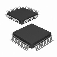
IC I/O EXPANDER 24B 44MQFP
Manufacturer
Intersil
Datasheet
1.CMS82C55AZ.pdf
(26 pages)
Specifications of IMQ82C55AZ96
Interface
Programmable
Number Of I /o
24
Interrupt Output
No
Voltage - Supply
4.5 V ~ 5.5 V
Operating Temperature
-40°C ~ 85°C
Mounting Type
Surface Mount
Package / Case
44-MQFP, 44-PQFP
Lead Free Status / RoHS Status
Lead free / RoHS Compliant
Frequency - Clock
-
Available stocks
Company
Part Number
Manufacturer
Quantity
Price
Company:

Part Number:
IMQ82C55AZ96
Manufacturer:
OKI
Quantity:
125


ACK - (Acknowledge Input). A “low” on this input informs the
82C55A that the data from Port A or Port B is ready to be
accepted. In essence, a response from the peripheral device
indicating that it is ready to accept data, (See Note 1).
INTR - (Interrupt Request). A “high” on this output can be
used to interrupt the CPU when an output device has
accepted data transmitted by the CPU. INTR is set when
ACK is a “one”, OBF is a “one” and INTE is a “one”. It is reset
by the falling edge of WR.
INTE A
Controlled by Bit Set/Reset of PC6.
INTE B
Controlled by Bit Set/Reset of PC2.
NOTE:
CONTROL WORD
D7
1. To strobe data into the peripheral device, the user must operate
1
the strobe line in a hand shaking mode. The user needs to send
OBF to the peripheral device, generates an ACK from the
peripheral device and then latch data into the peripheral device
on the rising edge of OBF.
D6
0
PERIPHERAL
INPUT FROM
D5
1
D4
1
INTR
STB
1/0
D3 D2 D1 D0
IBF
RD
PC6, PC7
1 = INPUT
0 = OUTPUT
RD
10
MODE 1 (PORT A)
INTE
A
MS82C55A, MQ82C55A, MP82C55A
PC6, PC7
PA7-PA0
tPS
tSIB
PC4
PC5
PC3
FIGURE 7. MODE 1 (STROBED INPUT)
tST
FIGURE 6. MODE 1 INPUT
2
8
STBA
IBFA
INTRA
I/O
tSIT
tPH
CONTROL WORD
D7 D6 D5 D4 D3 D2 D1 D0
CONTROL WORD
D7
CONTROL WORD
D7 D6 D5 D4 D3 D2 D1 D0
1
1
1
D6
0
D5
1
tRIT
D4
1
1/0
D3 D2 D1 D0
FIGURE 8. MODE 1 OUTPUT
1
1
PC4, PC5
1 = INPUT
0 = OUTPUT
WR
WR
1
0
RD
tRIB
MODE 1 (PORT B)
MODE 1 (PORT A)
MODE 1 (PORT B)
INTE
INTE
INTE
B
A
B
PC4, PC5
PB7-PB0
PB7-PB0
PA7-PA0
PC7
PC6
PC3
PC1
PC2
PC0
PC2
PC1
PC0
June 15, 2006
2
8
8
FN6140.2
8
STBB
IBFB
INTRB
OBFA
ACKA
INTRA
OBFB
ACKB
INTRB
Related parts for IMQ82C55AZ96
Image
Part Number
Description
Manufacturer
Datasheet
Request
R

Part Number:
Description:
Intersil Corporation [CMOS Serial Controller Interface]
Manufacturer:
Intersil Corporation
Datasheet:
Part Number:
Description:
Manufacturer:
Intersil Corporation
Datasheet:
Part Number:
Description:
357-036-542-201 CARDEDGE 36POS DL .156 BLK LOPRO
Manufacturer:
Intersil Corporation
Datasheet:
Part Number:
Description:
1024-Word x 4-Bit LSI Static RAM
Manufacturer:
Intersil Corporation
Datasheet:
Part Number:
Description:
General Purpose NPN Transistor Arrays FN341.4
Manufacturer:
Intersil Corporation
Datasheet:
Part Number:
Description:
CMOS 16-Bit Microprocessor
Manufacturer:
Intersil Corporation
Datasheet:
Part Number:
Description:
Manufacturer:
Intersil Corporation
Datasheet:
Part Number:
Description:
Manufacturer:
Intersil Corporation
Datasheet:
Part Number:
Description:
Manufacturer:
Intersil Corporation
Datasheet:
Part Number:
Description:
Manufacturer:
Intersil Corporation
Datasheet:
Part Number:
Description:
CMOS 6-Bit Latch and Decoder Memory Interfaces
Manufacturer:
Intersil Corporation
Datasheet:
Part Number:
Description:
CA3046General Purpose NPN Transistor Arrays
Manufacturer:
Intersil Corporation
Datasheet:
Part Number:
Description:
Manufacturer:
Intersil Corporation
Datasheet:
Part Number:
Description:
TR909 DLC/FLC SLIC with Low Power Standby
Manufacturer:
Intersil Corporation
Datasheet:
Part Number:
Description:
Manufacturer:
Intersil Corporation
Datasheet: