SI3015-F-FS Silicon Laboratories Inc, SI3015-F-FS Datasheet
SI3015-F-FS
Specifications of SI3015-F-FS
Available stocks


Related parts for SI3015-F-FS


SI3015-F-FS Summary of contents
Page 1
... C1A 4 VD3.3 5 ISOB 20 GND 19 6 VD3.3 VDA 7 18 GND RTS/ VDB 16 9 EESD/D2 RXD/ RI/D1 TXD/WR 14 INT/D0 CTS/ AOUT/INT 12 RESET Si3015 QE2 1 16 FILT2 DCT 2 15 FILT IGND C1B 4 13 REXT RNG1 12 5 REXT2 RNG2 11 6 REF VREG2 VREG Patents pending ...
Page 2
Si2403 2 Rev. 1.2 ...
Page 3
... S-Registers . . . . . . . . . . . . . . . . . . . . . . . . . . . . . . . . . . . . . . . . . . . . . . . . . . . . . . . . . . . . . 33 6. User-Access Registers (U-Registers 6.1. Bit-Mapped U-Register Detail (Defaults in Bold .41 7. Parallel Interface Registers . . . . . . . . . . . . . . . . . . . . . . . . . . . . . . . . . . . . . . . . . . . . . . . .58 8. Pin Descriptions: Si2403 . . . . . . . . . . . . . . . . . . . . . . . . . . . . . . . . . . . . . . . . . . . . . . . . . .60 9. Pin Descriptions: Si3015 . . . . . . . . . . . . . . . . . . . . . . . . . . . . . . . . . . . . . . . . . . . . . . . . . .62 10. Ordering Guide . . . . . . . . . . . . . . . . . . . . . . . . . . . . . . . . . . . . . . . . . . . . . . . . . . . . . . . . . 64 11. Package Outline: 24-Pin TSSOP . . . . . . . . . . . . . . . . . . . . . . . . . . . . . . . . . . . . . . . . . . . 65 12. Package Outline: 16-Pin SOIC . . . . . . . . . . . . . . . . . . . . . . . . . . . . . . . . . . . . . . . . . . . . . 66 Document Change List . . . . . . . . . . . . . . . . . . . . . . . . . . . . . . . . . . . . . . . . . . . . . . . . . . . . .67 Contact Information . . . . . . . . . . . . . . . . . . . . . . . . . . . . . . . . . . . . . . . . . . . . . . . . . . . . . . . .68 Rev ...
Page 4
... The Si2403 specifications are guaranteed when the typical application circuit (including component tolerance) and any Si2403 and any Si3015 are used. See "Typical Application Schematic" on page 11. 2. All minimum and maximum specifications are guaranteed and apply across the recommended operating conditions. ...
Page 5
Table 2. DAA Loop Characteristics (V = 3 °C for K-Grade D A Parameter DC Termination Voltage DC Termination Voltage DC Termination Voltage DC Termination Voltage DC Termination Voltage DC Termination Voltage ...
Page 6
... Si2403 Si3015 Figure 1. Test Circuit for Loop Characteristics Table 3. DC Characteristics 3 °C for K-Grade Parameter High Level Input Voltage Low Level Input Voltage High Level Output Voltage Low Level Output Voltage Input Leakage Current Pullup Resistance Pins 11, 13, 14, 16, 23, 24 ...
Page 7
Table 4. DAA AC Characteristics (V = 3 °C for K-Grade Parameter Sample Rate Crystal Oscillator Frequency Transmit Frequency Response Receive Frequency Response 1 Transmit Full Scale Level 1 Receive ...
Page 8
Si2403 Table 5. Absolute Maximum Ratings Parameter DC Supply Voltage Input Current, Si2403 Digital Input Pins Digital Input Voltage CLKIN/XTALI Input Voltage Operating Temperature Range Storage Temperature Range Note: Permanent device damage may occur if the above Absolute Maximum Ratings ...
Page 9
UART Time for Modem Receive Path (8N1 Mode) 8-B it Data M ode tart RTS UART Timing for Modem Transmit Path (9N1 Mode with 9th Bit Escape) 9-B it ...
Page 10
Si2403 t CSS ADDRESS = RLDD D[7:0] t CSS ADDRESS = D[7: CSH ...
Page 11
Typical Application Schematic + R15 R7 R8 R16 R17 R19 Rev. 1.2 Si2403 11 ...
Page 12
... C25, must also be rated to greater than the surge voltage. Y-class capacitors are recommended for highest surge survival. 2. For FCC-only designs, C14, C38, C39, R12, R13, R31, and R32 are not required (leave Si3015 pin 12 unconnected); L1 and L2 may be replaced with a short; R2 may be ±5%; with Z1 rated may be rated also see Note 9. ...
Page 13
... C25, must also be rated to greater than the surge voltage. Y-class capacitors are recommended for highest surge survival. 2. For FCC-only designs, C14, C38, C39, R12, R13, R31, and R32 are not required (leave Si3015 pin 12 unconnected); L1 and L2 may be replaced with a short; R2 may be ±5%; with Z1 rated may be rated also see Note 9. ...
Page 14
Si2403 Item Data Rate 2400 bps 1200 bps 300 bps 300 bps Data Format Bit asynchronous Compatibility Operating Mode Switched network Data Modulation 2400 bps 1200 bps 0 to 300 bps Answer Tone ITU-T V.22bis, V.22, and V.21 modes Bell ...
Page 15
Table 7. Protocol Characteristics (Continued) Item Carrier Detect (level for ITU-T V.22bis, V.22, V.21, 212, 103) in Switched Network Hysteresis DTE Interface Line Equalization Connection Options Phone Types Dialing DTMF Output Level Pulse Dial Ratio Ring Cadence Call Progress Monitor ...
Page 16
Si2403 4. Functional Description The ISOmodem® chipset is a complete embedded- modem chipset with integrated arrangement (DAA) that provides a programmable line interface to meet global telephone line requirements. Available in two small packages, this solution includes a DSP data ...
Page 17
Command Mode Upon reset, the ISOmodem® chipset is in command mode and accepts “AT” commands. An outgoing modem call can be made using the “ATDT#” (tone dial) or “ATDP#” (pulse dial) command after the device is configured. If the ...
Page 18
Si2403 4.8. Error Correction The ISOmodem® chipset can employ error-correction (reliable) protocols to ensure error-free delivery of asynchronous data sent between the host and the remote end. The Si2403 supports V.42 and MNP2-4 error correction protocols. V.42 (LAPM) is most ...
Page 19
LVC S BITS Figure 6. Loop Voltage 30 ...
Page 20
Si2403 4.12. Overcurrent Detection The ISOmodem® chipset includes an overcurrent detection feature that measures the loop current at a programmable time after the Si2403 goes off-hook. This allows the Si2403 to detect connected to an improper telephone ...
Page 21
Table 8. Basic AT Command Set (Command Defaults in Bold) Command $ Display AT command mode settings. A Answer incoming call. A/ Re-execute last command. This is the only command not preceded by “AT” or followed by a <CR>. Dn ...
Page 22
... I0 Display Si2403 revision code. B: Revision B C: Revision C, etc. I1 Display Si2403 firmware revision code (numeric). I3 Display line-side revision code. 15F Si3015 Revision Display the Si2403 model number. “2403” Si2403 = I7 Diagnostic Results 1. See “AN70: Si2456/Si2433/Si2414/Si2403 Modem Designer’s Guide” for details. ...
Page 23
Table 8. Basic AT Command Set (Command Defaults in Bold) (Continued) Command X5 Extended results—Full CPM enabled including ringback detection. Adds ringback detection to X4 mode. Yn Long space disconnect—Modem hangs up after 1.5 seconds or more of continuous space ...
Page 24
Si2403 Table 8. Basic AT Command Set (Command Defaults in Bold) (Continued) Command +GCI = X Country settings - Automatically configure all registers for a particular country. X Country 0 Japan 9 Australia A Austria F Belgium 16 Brazil 1B ...
Page 25
Table 8. Basic AT Command Set (Command Defaults in Bold) (Continued) Command +VCDT = X Caller ID Type. X Mode 0 After ring only 1 Always Japan +VCID = X Caller ID Enable. X Mode 0 ...
Page 26
... DSP (Si2403), DAA interface section (Si2403), isolation interface (Si3015), and analog hybrid circuit (Si3015). Si2403 echoes data from TX pin (Register 0 in parallel mode) back to RX pin (Register 0 in parallel mode). Phone line termination required as in Figure test only the link operation, the hybrid and AFE codec can be removed from the test loop by setting the DL bit (U62, bit 1). & ...
Page 27
Table 9. Extended AT& Command Set (Command Defaults in Bold) (Continued) Command &T5 Initiate transmit as answering modem with automatic data generation. Modulation, data rate, and symbol rate are set by &H, &G, and S41. Data pattern is set by ...
Page 28
Si2403 Table 10. Extended AT% Command Set (Command Defaults in Bold) Command %$ Display AT% command settings. %B Report blacklist. See also S42 register. %On Answer mode %O1 Si2403 will auto-answer a call in answer mode %O2 Si2403 will auto-answer ...
Page 29
Table 11. Extended AT\ Command Set (Command Defaults in Bold) Command \$ Display AT\ command settings. \Bn Character length will be automatically set in autobaud mode. \B0 6N1—six data bits, no parity, one stop bit, one start bit, eight bits ...
Page 30
Si2403 Table 11. Extended AT\ Command Set (Command Defaults in Bold) (Continued) Command \Q3 Use RTS/CTS \Q4 Use XON/XOFF flow control for modem-to-DTE interface. Does not enable modem-to-modem flow control. \Tn DTE rate - Change DTE rate. When changing rates, ...
Page 31
Table 11. Extended AT\ Command Set (Command Defaults in Bold) (Continued) Command \U Serial mode—causes a low pulse (25 ms and DCD. INT to be the inverse of ESC. RTS to be the inverse of CTS. Parallel mode—causes ...
Page 32
Si2403 2 Meaning Numeric 0 Command was successful 1 Link established at 300 bps or higher 2 Incoming ring detected 3 Link dropped 4 Command failed 5 Link establish at 1200 6 Dial tone not present 7 Line busy 9 ...
Page 33
S-Registers The S command allows reading (Sn?) or writing (Sn=x) the S-registers. The S-registers store values for functions that, typically, are rarely changed, such as timers or counters, and the ASCII values of control characters, such as carriage return. ...
Page 34
Si2403 Table 13. S-Register Descriptions (Continued) S-Register (Decimal) 30 Disconnect Activity Timer—Sets the length of time that the modem stays online before disconnecting with no activity on the serial port, parallel port, or telephone line (Ring, hookswitch flash, or caller ...
Page 35
User-Access Registers (U-Registers) The :U AT command is used to write these 16-bit U-registers, and the :R command is used to read them. U- registers are identified by a hexidecimal (hex) address. Register Name Description U00 DT1A0 DT1 registers ...
Page 36
Si2403 Table 14. U-Register Descriptions (Continued) Register Name Description U17 BT1A0 BT1 registers set the coefficients for stage 1 of the Busy Tone Detect filter. Default is for FCC countries. See AN70 for other country settings. U18 BT1B1 U19 BT1B2 ...
Page 37
Table 14. U-Register Descriptions (Continued) Register Name Description U35 DMOT Minimum dialtone on time in seconds multiplied by 7200. U37 PD0 Number of pulses to dial 0. U38 PD1 Number of pulses to dial 1. U39 PD2 Number of pulses ...
Page 38
Si2403 Table 14. U-Register Descriptions (Continued) Register Name Description U51 LCDF Loop current debounce off time (ms units). U52 XMTL Transmit level (1 dB units)—Sets the modem data pump transmitter level. Default level of 0 corresponds to –9.85 dBm. Transmit ...
Page 39
Table 15. Bit-Mapped U-Register Summary Reg. Name Bit Bit Bit Bit U4D MOD1 TOCT NHFP U53 MOD2 REV U62 DAAC1 U65 DAAC4 PWM PWMG PDN U66 DAAC5 U67 ITC1 U68 ITC2 U69 ITC3 U6A ITC4 U6E CK1 ...
Page 40
Si2403 6.1. Bit-Mapped U-Register Detail (Defaults in Bold) U4D MOD1 Bit D15 D14 D13 D12 Name TOCT NHFP NHFD CLPD Type R/W R/W Reset settings 0x0000 = Bit Name 15 Reserved Read returns zero. 14 TOCT Turn Off Calling Tone. ...
Page 41
Bit Name 1 LLC Low Loop Current Detect (required for CTR21 Disabled. 1 Enabled LCN Loop Current Needed No. 1 Yes. = U53 MOD2 Bit D15 D14 D13 D12 Name REV Type R/W Reset ...
Page 42
... Si2433/Si2414/Si2403 Modem Designer’s Guide”. 14 PWMG PWM Gain gain gain applied to AOUT PDN Powerdown. Completely powerdown the Si2403 and Si3015. Once set to 1, the Si2403 must be reset to power on Normal. 1 Powerdown. = 12:8 Reserved Read returns zero. 7:5 Reserved Must not change in a read-modify-write. 4 PDL* Powerdown Line-Side Chip ...
Page 43
U66 DAAC5 Bit D15 D14 D13 D12 Name Type Reset settings 0x0049 = Bit Name 15:7 Reserved Read returns zero. 6 FDT* Frame Detect. 0 Indicates isolation link has not established frame lock Indicates isolation link frame lock ...
Page 44
Si2403 U67 ITC1 Bit D15 D14 D13 D12 D11 Name Type Reset settings 0x0008 = Bit Name 15:8 Reserved Read returns zero. 7 OFF DC Termination Off Normal operation. The OFF bit must always be set to 0 ...
Page 45
U68 ITC2 Bit D15 D14 D13 D12 Name Type Reset settings 0x0000 = Bit Name 15:8 Reserved Read returns zero. 7:5 Reserved Do not modify. 4 LIM Current Limit All other modes. 1 CTR21 mode Reserved ...
Page 46
Si2403 U69 ITC3 Bit D15 D14 D13 D12 D11 D10 Name Type Reset settings 0x0006 = Bit Name 15:8 Reserved Read returns zero. 7 Reserved Do not modify. Must be set to zero. 6 DIAL DTMF Dialing Mode. This bit ...
Page 47
U6A ITC4 Bit D15 D14 D13 D12 Name Type Reset settings N/A = Bit Name 15:3 Reserved Read returns zero. 2 OVL Overload Detected. This bit has the same function as ROV but clears itself after the overload has been ...
Page 48
Si2403 U6F PTMR Bit D15 D14 D13 D12 Name Type Reset settings 0x00FF = Bit Name 15:8 Reserved Do not modify 7:0 PTMR[7:0] Parallel Port Receive FIFO Interrupt Timer (msec units). See “AN70: Si2456/Si2433/Si2414/ Si2403 Modem Designer’s Guide” for more ...
Page 49
U70 IO0 Bit D15 D14 D13 D12 Name HES TES CIDM OCDM PPDM RIM DCDM Type R/W R/W R/W Reset settings 0x2700 = Bit Name 15 HES Hardware Escape Pin Disable. 1 Enable Reserved Read returns ...
Page 50
Si2403 U76 GEN1 Bit D15 D14 D13 D12 Name OHSR[6:0] Type R/W Reset settings 0x3240 = Bit Name 15:9 OHSR[6:0] Off-Hook Sample Rate (40 ms units) Sets the sample rate for the off-hook intrusion algorithms (1 second default). 8 FACL ...
Page 51
U77 GEN2 Bit D15 D14 D13 D12 Name IST[3:0] Type R/W Reset settings 0x401E = Bit Name 15:12 IST[3:0] Intrusion Settling Time (250 ms units). Delay between the time the Si2403 goes off-hook and the time the off-hook intrusion algo- ...
Page 52
Si2403 U78 GEN3 Bit D15 D14 D13 D12 Name IB[1:0] Type R/W Reset settings 0x0000 = Bit Name 15:14 IB[1:0] Intrusion Blocking. Defines the method used to block the off-hook intrusion algorithm from operation after dialing has begun ...
Page 53
U79 GEN4 Bit D15 D14 D13 D12 Name Type Bit Name 15:5 Reserved Read returns zero. 4:0 LVCS[4:0] Line Voltage Current Sense. Represents either the line voltage, loop current, or on-hook line monitor depending on the state of the MODE, ...
Page 54
Si2403 U7A GENA Bit D15 D14 D13 D12 D11 D10 Name Type Reset settings 0x0000 = Bit Name 15:8 Reserved Read returns to zero. 7 DOP Dial or Pulse Normal ATDTW operation 1 Use ATDTW for Pulse/Tone Dial ...
Page 55
U7C GENC Bit D15 D14 D13 D12 D11 D10 Name Type Reset settings 0x0000 = Bit Name 15:5 Reserved Reads returns to zero. 4 RIGPO RI. RI (pin 15), follows this bit when RIGPIOEN 3:1 Reserved Reads returns to zero. ...
Page 56
Si2403 U7D GEND Bit D15 D14 D13 D12 D11 D10 LVFE Name R/W Type Reset settings 0x0000 = Bit Name 15:14 Reserved Reads returns to zero. 13 LVFE LVCS Filter Enable Normal operation 1 = Enables optional filtering ...
Page 57
Parallel Interface Registers Parallel Interface 0 (0x00) Bit Name Type Reset settings 0x00 = Bit Name 7:0 TX/RX Parallel Interface Transmit/Receive. This register functions similarly to the serial port TX pin on writes to the parallel ...
Page 58
Si2403 Parallel Interface 1 (0x01) Bit Name RXF TXE REM Type Reset settings 0110_0011 = Bit Name 7 RXF Receive FIFO Almost Full (status). Receive FIFO (12 deep) contains three or more empty locations ...
Page 59
Pin Descriptions: Si2403 Pin # Pin Name 1 CLKIN/XTALI Clock Input/Crystal Oscillator Pin. This pin provides support for parallel-resonant, AT-cut crystals. XTALI also acts as an input in the event that an external clock source is used in place ...
Page 60
Si2403 Pin # Pin Name 10 TXD/WR Transmit Data/Write Enable. Data input from DTE TXD pin in serial mode. Active low write-enable pin in paral- lel mode. 11 CTS/CS Clear-to-Send/Chip Select. Active low clear-to-send (for flow control) in serial mode. ...
Page 61
... Pin Descriptions: Si3015 Pin # Pin Name 1 QE2 Transistor Emitter 2. Connects to the emitter of Q4. 2 DCT DC Termination. Provides dc termination to the telephone network. 3 IGND Isolated Ground. Connects to ground on the line-side interface. Also connects to capacitor C2. 4 C1B Isolation Capacitor 1B. Connects to one side of isolation capacitor C1. ...
Page 62
Si2403 Pin # Pin Name 13 REXT External Resistor. Sets the real ac termination impedance Receive Input. Serves as the receive side input from the telephone network. 15 FILT Filter. Provides filtering for the dc termination circuits. 16 ...
Page 63
... Ordering Guide Chipset Description Si2403 Commercial Si2403 Commercial Pb-free Digital Line Si2403-KT Si3015-KS Si2403-FT Si3015-F-FS Rev. 1.2 Si2403 Temperature ° °C 63 ...
Page 64
Si2403 11. Package Outline: 24-Pin TSSOP Figure 8 illustrates the package details for the Si2403. Table 16 lists the values for the dimensions shown in the illustration. D γ Figure 8. 24-Pin Thin Shrink Small Outline Package (TSSOP) Table 16. ...
Page 65
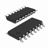
... Package Outline: 16-Pin SOIC Figure 9 illustrates the package details for the Si3015. Table 17 lists the values for the dimensions shown in the illustration Seating Plane Figure 9. 16-pin Small Outline Integrated Circuit (SOIC) Package Table 17. Package Diagram Dimensions E H θ Detail γ Millimeters ...
Page 66
Si2403 OCUMENT HANGE IST Revision 1.0 to Revision 1.1 Updated "Functional Block Diagram" on page 1. Updated Table 6 on page 8. Expanded “+GCI country codes” in Table 8 on page 21. Updated S-registers S43 and S44 ...
Page 67
N : OTES Rev. 1.2 Si2403 67 ...
Page 68
... Should Buyer purchase or use Silicon Laboratories products for any such unintended or unauthorized ap- plication, Buyer shall indemnify and hold Silicon Laboratories harmless against all claims and damages. Silicon Laboratories, Silicon Labs, and ISOmodem are trademarks of Silicon Laboratories Inc. Other products or brandnames mentioned herein are trademarks or registered trademarks of their respective holders. ...