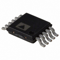
AD7150BRMZ Analog Devices Inc, AD7150BRMZ Datasheet - Page 16

AD7150BRMZ
Manufacturer Part Number
AD7150BRMZ
Description
IC CAP CONV 2CH ULT LP 10MSOP
Manufacturer
Analog Devices Inc
Type
Capacitance-to-Digital Converterr
Datasheet
1.AD7150BRMZ.pdf
(28 pages)
Specifications of AD7150BRMZ
Design Resources
Using AD7150 for Proximity Sensing Appls (CN0095)
Input Type
Voltage
Output Type
Digital
Interface
2-Wire Serial
Current - Supply
120µA
Mounting Type
Surface Mount
Package / Case
10-MSOP, Micro10™, 10-uMAX, 10-uSOP
Resolution (bits)
12bit
Data Interface
2-Wire, I2C, Serial
Supply Voltage Range - Analog
2.7V To 3.6V
Supply Current
100µA
Digital Ic Case Style
SOP
No. Of Pins
10
Lead Free Status / RoHS Status
Lead free / RoHS Compliant
For Use With
EVAL-AD7150EBZ - BOARD EVAL FOR AD7150
Lead Free Status / RoHS Status
Lead free / RoHS Compliant, Lead free / RoHS Compliant
Available stocks
Company
Part Number
Manufacturer
Quantity
Price
Company:
Part Number:
AD7150BRMZ
Manufacturer:
ADI
Quantity:
1 000
Company:
Part Number:
AD7150BRMZ
Manufacturer:
ADI
Quantity:
103
Company:
Part Number:
AD7150BRMZ-REEL
Manufacturer:
ON
Quantity:
4 300
Company:
Part Number:
AD7150BRMZ-REEL
Manufacturer:
ADI
Quantity:
1 000
Part Number:
AD7150BRMZ-REEL
Manufacturer:
ADI/亚德诺
Quantity:
20 000
AD7150
DATA REGISTERS
Ch1 Address Pointer 0x01, 0x02
Ch2 Address Pointer 0x03,0x04
16 Bits, Read-Only, Default Value 0x0000
Data from the last complete capacitance-to-digital conversion
reflects the capacitance on the input. Only the 12 MSBs (most
significant bits) of the data registers are used for the CDC
result. The 4 LSBs (least significant bits) are always 0, as shown
in Figure 36.
The nominal AD7150 CDC transfer function (an ideal transfer
function excluding offset and/or gain error) maps the input
capacitance between zero scale and full scale to output data
codes between 0x3000 and 0xCFF0 only (see Table 8).
Table 8. AD7150 Capacitance-to-Data Mapping
Data
0x0000
0x3000
0x8000
0xCFF0
0xFFF0
The input capacitance can be calculated from the output data
using the following equation:
where Input_Range = 4 pF, 2 pF, 1 pF, or 0.5 pF.
The following is the same equation written with hexadecimal
numbers:
A data register is updated after a finished conversion on the
capacitive channel, with one exception: when the serial interface
read operation from the data register is in progress, the data
register is not updated and the new capacitance conversion
result is lost.
The stop condition on the serial interface is considered to be the
end of the read operation. Therefore, to prevent incorrect data
reading through the serial interface, the two bytes of a data
register should be read sequentially using the register address
pointer auto-increment feature of the serial interface.
MSB
BIT 7 BIT 6 BIT 5 BIT 4 BIT 3 BIT 2
C
C
DATA HIGH
(
(
pF
pF
)
)
=
=
Data
Data
0
40944
9 x
−
−
12-BIT CDC RESULT
Input Capacitance
Not valid, underrange
Zero-scale (0 pF)
Mid-scale (+1 pF)
Full-scale (+2 pF)
Not valid, overrange
Figure 36. CDC Data Register
12288
FF
x 0
3000
0
BIT 1 BIT 0 BIT 7 BIT 6 BIT 5 BIT 4 BIT 3 BIT 2
×
×
Input
Input
_
_
Range
Range
DATA LOW
0
BIT 1 BIT 0
Rev. 0 | Page 16 of 28
LSB
AVERAGE REGISTERS
Ch1 Address Pointer 0x05, 0x06
Ch2 Address Pointer 0x07,0x08
16 Bits, Read-Only, Default Value 0x0000
These registers show the average calculated from the previous
CDC data. The 12-bit CDC result corresponds to the 12 MSBs
of the average register.
The settling time of the average can be set by programming the
ThrSettling bits in the setup registers. The average register is
overwritten directly with the CDC output data, that is, the
history is forgotten if the timeout is enabled and elapses.
FIXED THRESHOLD REGISTERS
Ch1 Address Pointer 0x09, 0x0A
Ch2 Address Pointer 0x0C,0x0D
16 Bits, Read/Write, Factory Preset 0x0886
A constant threshold for the output comparator in the fixed
threshold mode can be set using these registers. The 12-bit
CDC result corresponds to the 12 MSBs of the threshold
register. The fixed threshold registers share the address pointer
and location on-chip with the sensitivity and timeout registers.
The fixed threshold registers are not accessible in the adaptive
threshold mode.
SENSITIVITY REGISTERS
Ch1 Address Pointer 0x09
Ch2 Address Pointer 0x0C
8 Bits, Read/Write, Factory Preset 0x08
Sensitivity registers set the distance of the positive threshold above
the data average, and the distance of the negative threshold below
the data average, in the adaptive threshold mode.
The sensitivity is an 8-bit value and is mapped to the lower eight
bits of the 12-bit CDC data, that is, it corresponds to the 16-bit
data register as shown in Figure 38.
BIT 7 BIT 6 BIT 5 BIT 4 BIT 3 BIT 2
Figure 38. Relation Between Sensitivity Register and CDC Data Register
DATA AVERAGE
DATA HIGH
THRESHOLD
THRESHOLD
NEGATIVE
POSITIVE
BIT 7 BIT 6 BIT 5 BIT 4 BIT 3
DATA
12-BIT CDC RESULT
OUTPUT ACTIVE
Figure 37. Threshold Sensitivity
BIT 1 BIT 0 BIT 7 BIT 6 BIT 5 BIT 4 BIT 3 BIT 2
SENSITIVITY
TIME
BIT 2 BIT 1 BIT 0
SENSITIVITY
SENSITIVITY
DATA LOW
BIT 1 BIT 0


