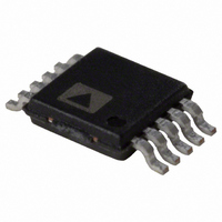
AD7150BRMZ Analog Devices Inc, AD7150BRMZ Datasheet - Page 4

AD7150BRMZ
Manufacturer Part Number
AD7150BRMZ
Description
IC CAP CONV 2CH ULT LP 10MSOP
Manufacturer
Analog Devices Inc
Type
Capacitance-to-Digital Converterr
Datasheet
1.AD7150BRMZ.pdf
(28 pages)
Specifications of AD7150BRMZ
Design Resources
Using AD7150 for Proximity Sensing Appls (CN0095)
Input Type
Voltage
Output Type
Digital
Interface
2-Wire Serial
Current - Supply
120µA
Mounting Type
Surface Mount
Package / Case
10-MSOP, Micro10™, 10-uMAX, 10-uSOP
Resolution (bits)
12bit
Data Interface
2-Wire, I2C, Serial
Supply Voltage Range - Analog
2.7V To 3.6V
Supply Current
100µA
Digital Ic Case Style
SOP
No. Of Pins
10
Lead Free Status / RoHS Status
Lead free / RoHS Compliant
For Use With
EVAL-AD7150EBZ - BOARD EVAL FOR AD7150
Lead Free Status / RoHS Status
Lead free / RoHS Compliant, Lead free / RoHS Compliant
Available stocks
Company
Part Number
Manufacturer
Quantity
Price
Company:
Part Number:
AD7150BRMZ
Manufacturer:
ADI
Quantity:
1 000
Company:
Part Number:
AD7150BRMZ
Manufacturer:
ADI
Quantity:
103
Company:
Part Number:
AD7150BRMZ-REEL
Manufacturer:
ON
Quantity:
4 300
Company:
Part Number:
AD7150BRMZ-REEL
Manufacturer:
ADI
Quantity:
1 000
Part Number:
AD7150BRMZ-REEL
Manufacturer:
ADI/亚德诺
Quantity:
20 000
AD7150
Parameter
POWER REQUIREMENTS
1
2
3
4
TIMING SPECIFICATIONS
V
Table 2.
Parameter
CONVERTER
SERIAL INTERFACE
1
2
3
4
5
6
Capacitance units: one picofarad (1 pF) = 1 × 10
The CAPDAC can be used to shift (offset) the input range. The total capacitance of the sensor can therefore be up to the sum of the CAPDAC value and the conversion
input range. With the autoCAPDAC feature, the CAPDAC is adjusted automatically when the CDC input value is lower than 25% or higher than 75% of the CDC
nominal input range.
Specification is not production tested but is supported by characterization data at initial product release.
Digital inputs equal to V
Specification is not production tested but is supported by characterization data at initial product release.
Wake-up time is the maximum delay between the last SCL edge writing the configuration register and the start of conversion.
Power-up time is the maximum delay between the V
command.
Reset time is the maximum delay between the last SCL edge writing the reset command and either the start of conversion or when ready to receive a serial interface
command.
Sample tested during initial release to ensure compliance.
All input signals are specified with input rise/fall times = 3 ns, measured between the 10% and 90% points. Timing reference points at 50% for inputs and outputs.
Output load = 10 pF.
DD
V
I
I
Conversion Time
Wake-Up Time from Power-Down Mode
Power-Up Time
Reset Time
SCL Frequency
SCL High Pulse Width, t
SCL Low Pulse Width, t
SCL, SDA Rise Time, t
SCL, SDA Fall Time, t
Hold Time (Start Condition), t
Setup Time (Start Condition), t
Data Setup Time, t
Setup Time (Stop Condition), t
Data Hold Time (Master), t
Bus-Free Time (Between Stop and Start Condition), t
DD
DD
DD
= 2.7 V to 3.6 V; GND = 0 V; Input Logic 0 = 0 V; Input Logic 1 = V
Current
Current Power-Down Mode
-to-GND Voltage
SDA
SCL
4
1, 4
1, 3
P
5, 6
t
BUF
SU;DAT
DD
F
or GND.
R
S
LOW
HIGH
t
HD;STA
HD;DAT
HD;STA
SU;STO
t
SU;STA
4
LOW
t
R
−12
t
HD;DAT
1, 2
farad (F); one femtofarad (1 fF) = 10
DD
crossing the minimum level (2.7 V) and either the start of conversion or when ready to receive a serial interface
Min
2.7
Figure 2. Serial Interface Timing Diagram
BUF
t
HIGH
t
F
t
SU;DAT
Rev. 0 | Page 4 of 28
Min
0
0.6
1.3
0.6
0.6
0.1
0.6
10
1.3
Typ
100
1
3
Typ
0.15
2
2
−15
Max
3.6
120
5
10
DD
farad (F).
; –40°C to +85°C, unless otherwise noted.
Max
10
400
0.3
0.3
S
Unit
V
μA
μA
μA
t
SU;STA
1
Unit
ms
ms
ms
ms
kHz
μs
μs
μs
μs
μs
μs
μs
μs
ns
μs
t
HD;STA
Test Conditions/Comments
Both channels, 5 ms per channel.
See Figure 2.
After this period, the first clock is generated.
Relevant for repeated start condition.
Test Conditions/Comments
V
Temperature ≤ 25°C
Temperature = 85°C
DD
= 3.3 V, nominal
t
SU;STO
P


