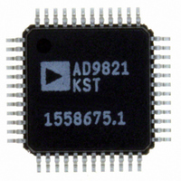
AD9821KSTZ Analog Devices Inc, AD9821KSTZ Datasheet - Page 11

AD9821KSTZ
Manufacturer Part Number
AD9821KSTZ
Description
IC IMAGE SGNL PROC 12BIT 48-LQFP
Manufacturer
Analog Devices Inc
Type
Image Sensorr
Datasheet
1.AD9821KST.pdf
(16 pages)
Specifications of AD9821KSTZ
Input Type
Logic
Output Type
Logic
Interface
3-Wire Serial
Mounting Type
Surface Mount
Package / Case
48-LQFP
Analog Front End Type
CCD
Analog Front End Category
Video
Interface Type
Serial (3-Wire)
Sample Rate
40MSPS
Input Voltage Range
0.5V
Operating Supply Voltage (min)
2.7V
Operating Supply Voltage (typ)
3.3V
Operating Supply Voltage (max)
3.6V
Resolution
12b
Number Of Adc's
1
Power Supply Type
Analog/Digital
Operating Temp Range
-20C to 85C
Operating Temperature Classification
Commercial
Mounting
Surface Mount
Pin Count
48
Package Type
LQFP
Number Of Channels
1
Lead Free Status / RoHS Status
Lead free / RoHS Compliant
Current - Supply
-
Lead Free Status / RoHS Status
Compliant, Lead free / RoHS Compliant
Available stocks
Company
Part Number
Manufacturer
Quantity
Price
CIRCUIT DESCRIPTION AND OPERATION
The AD9821 signal processing chain is shown in Figure 10.
Each processing step is essential in achieving a high quality
image from the raw imager pixel data.
Differential Input SHA
The differential input SHA circuit is designed to accommodate
a variety of different image sensor output voltages. The timing
shown in Figure 8 illustrates how the DATACLK signal is used to
sample both the VIN+ and VIN– signals simultaneously. The
imager signal is sampled on the rising edges of DATACLK.
Placement of this clock signal is critical in achieving the best
performance from the imager. An internal DATACLK delay (t
of 3 ns is caused by internal propagation delays.
The differential input can be used in a variety of single-ended
and differential configurations, as shown in Table VI. The
allowable voltage range for both VIN+ or VIN– is from 0 V
to 1.8 V. Signal levels outside this range will result in severely
degraded performance. Regardless of the input configuration,
the voltage sampled by the SHA is always equal to VIN+ minus
VIN–. VIN+ must always be equal to or greater than VIN– or
REV. 0
0.1 F
VIN+
VIN–
BYP1
0.45V
INTERNAL
SHA
BIAS
Figure 10. Internal Block Diagram
REGISTER
0dB TO 36dB
VGA GAIN
VGA
10
DATACLK
ID
)
–11–
8-BIT
DAC
negative clipping will occur. A small amount of offset between
the VIN+ and VIN– signals is allowable and can be corrected by
the Optical Black Clamp, up to ± 30 mV.
Note that the VIN+ and VIN– inputs do not contain any dc
restoration or bias circuitry. Therefore, dc-coupling is recom-
mended when driving the AD9821 analog inputs. If ac-coupling is
used, external biasing circuitry must be provided for the VIN+
and VIN– inputs to keep them in the acceptable common-mode
voltage range of 0 V to 1.8 V.
VIN+ Range (V) VIN– Range (V) SHA Output Range (V)
Black White
0
0.5
1.0
0.5
1.0
FILTERING
DIGITAL
OPTICAL BLACK
Table VI. Example Input Voltage Configurations
1.0
1.5
1.5
1.0
1.0
CLAMP
12-BIT
ADC
REFB
1.0V
INTERNAL
Black White
0
0.5
1.0
0.5
1.0
1.0 F 1.0 F
VREF
CLAMP LEVEL
REGISTER
REFT
2.0V
8
0
0.5
0.5
0
0
12
Black
0
0
0
0
0
PBLK
DOUT
CLPOB
AD9821
White
1.0
1.0
1.0
1.0
1.0


