LM2502SQ/NOPB National Semiconductor, LM2502SQ/NOPB Datasheet - Page 23
LM2502SQ/NOPB
Manufacturer Part Number
LM2502SQ/NOPB
Description
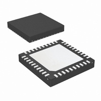
IC SER/DESER MPL DISPL 40-LLP
Manufacturer
National Semiconductor
Series
LMr
Datasheet
1.LM2502SMNOPB.pdf
(27 pages)
Specifications of LM2502SQ/NOPB
Function
Serializer/Deserializer
Data Rate
307Mbps
Input Type
LVCMOS
Output Type
LVCMOS
Number Of Inputs
22
Number Of Outputs
3
Voltage - Supply
1.7 V ~ 3.3 V
Operating Temperature
-30°C ~ 85°C
Mounting Type
Surface Mount
Package / Case
40-LLP
Lead Free Status / RoHS Status
Lead free / RoHS Compliant
Other names
LM2502SQTR


Application Information
DISPLAY APPLICATION
The LM2502 chipset is intended for Interface between a host
(processor) and a Display. It supports a 16 or 8-bit CPU style
interface and can be configured for i80 or m68 modes.
The Master side connection is shown in Figure 19. Input
Clock frequency and the selection of the PLL_CON setting
are determined by system parameters. These include the
required display bandwidth, the Master load rate and the
Display Driver input timing requirements. See the System
Considerations section for more details.
The Display side parallel bus may be connected to one or
two displays. Each display has its own chipselect signal. If
only one display is required, the unused CS signal should be
tied HIGH (V
open on the Slave. The Slave provides an optional clock
DDIO
) on the Master, and the unused output left
FIGURE 18. LM2502 UFBGA Package PWR (V
(Continued)
23
output. If this is desired the CLKDIS
tied HIGH. A different PLL_CON setting can be used to alter
the frequency if desired. As the Divisor setting in the Slave is
not used for data recovery. For the dual display application,
the multidrop bus should be laid out to minimize any result-
ing stub lengths on the Data, A/D, and control signals.
If required, the Slave output clock can be enabled to provide
a output frequency reference. The frequency can be ad-
justed by setting different PLL_CON (divisor) settings (on the
Slave). This can then be used as a frequency reference
signal to the display module or other subsystem (ie camera
module). If the CLK output is not needed, tie the Slave
CLKDIS
ever the MPL link is enabled.
DD
*
pin Low to disable it. The Clock is available when
) and GND (V
SS
) Balls
20093321
*
pin needs to be also
www.national.com
Related parts for LM2502SQ/NOPB
Image
Part Number
Description
Manufacturer
Datasheet
Request
R

Part Number:
Description:
National Semiconductor [8-Bit D/A Converter]
Manufacturer:
National Semiconductor
Datasheet:
Part Number:
Description:
National Semiconductor [Media Coprocessor]
Manufacturer:
National Semiconductor
Datasheet:
Part Number:
Description:
Digitally Controlled Tone and Volume Circuit with Stereo Audio Power Amplifier, Microphone Preamp Stage and National 3D Sound
Manufacturer:
National Semiconductor
Datasheet:
Part Number:
Description:
Digitally Controlled Tone and Volume Circuit with Stereo Audio Power Amplifier, Microphone Preamp Stage and National 3D Sound
Manufacturer:
National Semiconductor
Datasheet:
Part Number:
Description:
AC97 Rev 2 Codec with Sample Rate Conversion and National 3D Sound
Manufacturer:
National Semiconductor
Part Number:
Description:
Manufacturer:
National Semiconductor
Datasheet:
Part Number:
Description:
Manufacturer:
National Semiconductor
Datasheet:
Part Number:
Description:
General Purpose, Low Voltage, Low Power, Rail-to-Rail Output Operational Amplifiers
Manufacturer:
National Semiconductor
Datasheet:
Part Number:
Description:
8-bit 20 MSPS flash A/D converter.
Manufacturer:
National Semiconductor
Datasheet:
Part Number:
Description:
Low Noise Quad Operational Amplifier
Manufacturer:
National Semiconductor
Datasheet:
Part Number:
Description:
Quad Differential Line Receivers
Manufacturer:
National Semiconductor
Datasheet:
Part Number:
Description:
Quad High Speed Trapezoidal? Bus Transceiver
Manufacturer:
National Semiconductor
Datasheet:
Part Number:
Description:
Dual Line Receiver
Manufacturer:
National Semiconductor
Datasheet:
Part Number:
Description:
TTL to 10k ECL Level Translator with Latch
Manufacturer:
National Semiconductor
Datasheet: