LM2502SQ/NOPB National Semiconductor, LM2502SQ/NOPB Datasheet - Page 8
LM2502SQ/NOPB
Manufacturer Part Number
LM2502SQ/NOPB
Description
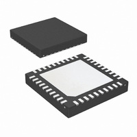
IC SER/DESER MPL DISPL 40-LLP
Manufacturer
National Semiconductor
Series
LMr
Datasheet
1.LM2502SMNOPB.pdf
(27 pages)
Specifications of LM2502SQ/NOPB
Function
Serializer/Deserializer
Data Rate
307Mbps
Input Type
LVCMOS
Output Type
LVCMOS
Number Of Inputs
22
Number Of Outputs
3
Voltage - Supply
1.7 V ~ 3.3 V
Operating Temperature
-30°C ~ 85°C
Mounting Type
Surface Mount
Package / Case
40-LLP
Lead Free Status / RoHS Status
Lead free / RoHS Compliant
Other names
LM2502SQTR


www.national.com
POWER UP TIMING(Note 5)
MPL POWER OFF TIMING
t
MASTER REFERENCE CLOCK (CLK)
f
t
CLK
t
PAZ
CLK
CP
T
Symbol
Symbol
Switching Characteristics
Over recommended operating supply and temperature ranges unless otherwise specified. (Note 2)
Recommended Input Timing Requirements
Over recommended operating supply and temperature ranges unless otherwise specified. (Note 2)
Note 1: “Absolute Maximum Ratings” are those values beyond which the safety of the device cannot be guaranteed. They are not meant to imply that the device
should be operated at these limits. The tables of “Electrical Characteristics” specify conditions for device operation.
Note 2: Typical values are given for VDDIO = 1.8V and VDD = VDDA = 3.0V and T
Note 3: Current into a device pin is defined as positive. Current out of device pins is defined as negative. Voltages are referenced to Ground unless otherwise
specified.
Note 4: UFBGA assumes 4 layer PCB, LLP assumes 2 layer PCB for thermal calculations.
Note 5: This parameter is Guaranteed by Design (GBD) based on simulation or bench characterization.
Note 6: This parameter is guaranteed by a ATE tester delay, actual turn off time is faster.
Note 7: Typical supply condition is V
Timing Diagrams
DC
Disable Time to Power
Down
Clock Frequency
Clock Period
Clock Duty Cycle
Clock Transition Times
(Rise or Fall, 20%–80%)
Parameter
Parameter
DDIO
= 1.8V and V
FIGURE 1. Serial Data Valid — Master to Slave
FIGURE 2. Slave Output Rise and Fall Time
Figure 7, This parameter is functionally
tested by the I
See Table 10
(Note 5)
DD
(Continued)
= V
DDA
= 3.0V, Maximum supply condition is V
Conditions
Conditions
DDZ
parameter. (Note 6)
8
A
= 25˚C.
DDIO
38.5
Min
Min
40
3
1
= V
20093318
DD
20093316
= V
DDA
Typ
Typ
50
= 3.3V for the I
Max
Max
333
50
26
60
14
DD
parameter.
Units
Units
MHz
ms
ns
ns
%
Related parts for LM2502SQ/NOPB
Image
Part Number
Description
Manufacturer
Datasheet
Request
R

Part Number:
Description:
National Semiconductor [8-Bit D/A Converter]
Manufacturer:
National Semiconductor
Datasheet:
Part Number:
Description:
National Semiconductor [Media Coprocessor]
Manufacturer:
National Semiconductor
Datasheet:
Part Number:
Description:
Digitally Controlled Tone and Volume Circuit with Stereo Audio Power Amplifier, Microphone Preamp Stage and National 3D Sound
Manufacturer:
National Semiconductor
Datasheet:
Part Number:
Description:
Digitally Controlled Tone and Volume Circuit with Stereo Audio Power Amplifier, Microphone Preamp Stage and National 3D Sound
Manufacturer:
National Semiconductor
Datasheet:
Part Number:
Description:
AC97 Rev 2 Codec with Sample Rate Conversion and National 3D Sound
Manufacturer:
National Semiconductor
Part Number:
Description:
Manufacturer:
National Semiconductor
Datasheet:
Part Number:
Description:
Manufacturer:
National Semiconductor
Datasheet:
Part Number:
Description:
General Purpose, Low Voltage, Low Power, Rail-to-Rail Output Operational Amplifiers
Manufacturer:
National Semiconductor
Datasheet:
Part Number:
Description:
8-bit 20 MSPS flash A/D converter.
Manufacturer:
National Semiconductor
Datasheet:
Part Number:
Description:
Low Noise Quad Operational Amplifier
Manufacturer:
National Semiconductor
Datasheet:
Part Number:
Description:
Quad Differential Line Receivers
Manufacturer:
National Semiconductor
Datasheet:
Part Number:
Description:
Quad High Speed Trapezoidal? Bus Transceiver
Manufacturer:
National Semiconductor
Datasheet:
Part Number:
Description:
Dual Line Receiver
Manufacturer:
National Semiconductor
Datasheet:
Part Number:
Description:
TTL to 10k ECL Level Translator with Latch
Manufacturer:
National Semiconductor
Datasheet: