LM2502SQ/NOPB National Semiconductor, LM2502SQ/NOPB Datasheet - Page 5
LM2502SQ/NOPB
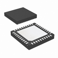
Manufacturer Part Number
LM2502SQ/NOPB
Description
IC SER/DESER MPL DISPL 40-LLP
Manufacturer
National Semiconductor
Series
LMr
Datasheet
1.LM2502SMNOPB.pdf
(27 pages)
Specifications of LM2502SQ/NOPB
Function
Serializer/Deserializer
Data Rate
307Mbps
Input Type
LVCMOS
Output Type
LVCMOS
Number Of Inputs
22
Number Of Outputs
3
Voltage - Supply
1.7 V ~ 3.3 V
Operating Temperature
-30°C ~ 85°C
Mounting Type
Surface Mount
Package / Case
40-LLP
Lead Free Status / RoHS Status
Lead free / RoHS Compliant
Other names
LM2502SQTR


POWER/GROUND PINS
Pin Name
Pin Descriptions
Note:
I = Input, O = Output, IO = Input/Output, V
Master Pinout - UFBGA Package
Slave Pinout - UFBGA Package
V
V
V
V
V
V
DDcore
SScore
DDIO
SSIO
DDA
SSA
SLV
MST
A
B
C
D
G
E
F
A
B
C
D
G
E
F
of Pins
No.
1
1
1
1
2
2
9
1
V
D10
D13
V
D0
D3
D6
DDIO
D8
D10
D13
1
D0
D3
D6
DDIO
D8
1
I/O, Type
Ground
Ground
Ground
Ground
Power
Power
Power
(Continued)
NC
DDIO
V
V
D11
D14
≤ V
D11
D14
D1
D4
D7
D9
SSIO
D1
D4
D7
D9
SSIO
2
2
DD
Power Supply Pin for the MPL Interface. 2.9V to 3.3V
Ground Pin for the MPL Interface, a low impedance ground path is required between
the Master and the Slave device - see Applications Information section.
Power Supply Pin for the digital core. 2.9V to 3.3V
Ground Pin for the digital core.
Power Supply Pin for the parallel interface. 1.7V to 3.3V
Ground Pin for the parallel interface.
Not Connected (C3-5, D3-5, E3-5). UFBGA Package only.
DAP = Ground. LLP Package only.
(V
DDA
= V
DDcore
D12
D15
D12
D15
NC
NC
NC
NC
NC
NC
D2
D5
D2
D5
3
3
Master (SER)
). Do not float input pins.
5
V
V
V
V
V
V
V
V
NC
NC
NC
NC
NC
NC
DDIO
DDIO
SSIO
SSIO
DDA
SSA
DDA
SSA
4
4
Description
CLKDIS*
INTR
M/S*
M/S*
MF0
MF0
A/D
A/D
NC
NC
NC
NC
NC
NC
5
5
PLLCON1
PLLCON0
PLLCON1
PLLCON0
V
V
Mode
Mode
CS2*
CS1*
CS2*
CS1*
MD1
MD0
SScore
SScore
Slave (DES)
6
6
PLLCON2
PLLCON2
V
V
www.national.com
MD0
MF1
MD1
MF1
DDcore
CLK
DDcore
CLK
PD*
PD*
MC
MC
7
7
Related parts for LM2502SQ/NOPB
Image
Part Number
Description
Manufacturer
Datasheet
Request
R

Part Number:
Description:
National Semiconductor [8-Bit D/A Converter]
Manufacturer:
National Semiconductor
Datasheet:
Part Number:
Description:
National Semiconductor [Media Coprocessor]
Manufacturer:
National Semiconductor
Datasheet:
Part Number:
Description:
Digitally Controlled Tone and Volume Circuit with Stereo Audio Power Amplifier, Microphone Preamp Stage and National 3D Sound
Manufacturer:
National Semiconductor
Datasheet:
Part Number:
Description:
Digitally Controlled Tone and Volume Circuit with Stereo Audio Power Amplifier, Microphone Preamp Stage and National 3D Sound
Manufacturer:
National Semiconductor
Datasheet:
Part Number:
Description:
AC97 Rev 2 Codec with Sample Rate Conversion and National 3D Sound
Manufacturer:
National Semiconductor
Part Number:
Description:
Manufacturer:
National Semiconductor
Datasheet:
Part Number:
Description:
Manufacturer:
National Semiconductor
Datasheet:
Part Number:
Description:
General Purpose, Low Voltage, Low Power, Rail-to-Rail Output Operational Amplifiers
Manufacturer:
National Semiconductor
Datasheet:
Part Number:
Description:
8-bit 20 MSPS flash A/D converter.
Manufacturer:
National Semiconductor
Datasheet:
Part Number:
Description:
Low Noise Quad Operational Amplifier
Manufacturer:
National Semiconductor
Datasheet:
Part Number:
Description:
Quad Differential Line Receivers
Manufacturer:
National Semiconductor
Datasheet:
Part Number:
Description:
Quad High Speed Trapezoidal? Bus Transceiver
Manufacturer:
National Semiconductor
Datasheet:
Part Number:
Description:
Dual Line Receiver
Manufacturer:
National Semiconductor
Datasheet:
Part Number:
Description:
TTL to 10k ECL Level Translator with Latch
Manufacturer:
National Semiconductor
Datasheet: