MAX9218ETM+ Maxim Integrated Products, MAX9218ETM+ Datasheet - Page 13
MAX9218ETM+
Manufacturer Part Number
MAX9218ETM+
Description
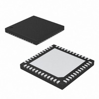
IC DESERIALIZER LVDS 48-TQFN
Manufacturer
Maxim Integrated Products
Datasheet
1.MAX9218ETMT.pdf
(15 pages)
Specifications of MAX9218ETM+
Function
Deserializer
Data Rate
700Mbps
Input Type
LVDS
Output Type
LVCMOS
Number Of Inputs
1
Number Of Outputs
27
Voltage - Supply
3 V ~ 3.6 V
Operating Temperature
-40°C ~ 85°C
Mounting Type
Surface Mount
Package / Case
48-TQFN Exposed Pad
Maximum Operating Temperature
+ 85 C
Minimum Operating Temperature
- 40 C
Mounting Style
SMD/SMT
Lead Free Status / RoHS Status
Lead free / RoHS Compliant


RGB_OUT[17:0] are grouped into three groups of six,
with each group switching about 1ns apart in the video
phase to reduce EMI and ground bounce.
CNTL_OUT[8:0] switch during the control phase. Output
transition times are slower in the 3MHz-to-7MHz and
7MHz-to-15MHz ranges and faster in the 15MHz-to-
35MHz range.
The MAX9218 deserializes video and control data at dif-
ferent times. Control data is deserialized during the video
blanking time. DE_OUT high indicates that video data is
being deserialized and output on RGB_OUT[17:0].
DE_OUT low indicates that control data is being deserial-
ized and output on CNTL_OUT[8:0]. When outputs are
not being updated, the last data received is latched on
the outputs. Figure 13 shows the DE_OUT timing.
There are separate on-chip power domains for digital
circuits and LVTTL/LVCMOS inputs (V
GND), outputs (V
(V
Figure 13. Output Timing
CCPLL
PCLK_OUT
CNTL_OUT
RGB_OUT
Staggered and Transition Time Adjusted
DE_OUT
Power-Supply Circuits and Bypassing
supply and V
Data Enable Output (DE_OUT)
______________________________________________________________________________________
CCO
= OUTPUT DATA HELD
CCPLL
supply and V
CONTROL DATA
GND), and the LVDS input
CCO
CC
DC-Balanced LVDS Deserializer
supply and
GND), PLL
Outputs
PCLK_OUT TIMING SHOWN FOR R/F = HIGH (RISING OUTPUT LATCH EDGE)
VIDEO DATA
(V
isolated by diode connections. Bypass each V
V
surface-mount ceramic 0.1µF and 0.001µF capacitors
in parallel as close to the device as possible, with the
smallest value capacitor closest to the supply pin. The
outputs are powered from V
1.71V to 3.6V supply, allowing direct interface to inputs
with 1.8V to 3.3V logic levels.
Interconnect for LVDS typically has a differential
impedance of 100Ω. Use cables and connectors that
have matched differential impedance to minimize
impedance discontinuities.
Twisted-pair and shielded twisted-pair cables offer
superior signal quality compared to ribbon cable and
tend to generate less EMI due to magnetic field cancel-
ing effects. Balanced cables pick up noise as common
mode, which is rejected by the LVDS receiver.
Separate the LVTTL/LVCMOS outputs and LVDS inputs
to prevent crosstalk. A four-layer PCB with separate lay-
ers for power, ground, and signals is recommended.
27-Bit, 3MHz-to-35MHz
CCO
CCLVDS
, V
CCPLL
supply and V
, and V
CCLVDS
CCLVDS
Cables and Connectors
CONTROL DATA
pin with high-frequency,
CCO
GND). The grounds are
, which accepts a
Board Layout
CC
13
,
Related parts for MAX9218ETM+
Image
Part Number
Description
Manufacturer
Datasheet
Request
R

Part Number:
Description:
Max9218 27-bit, 3mhz-to-35mhz Dc-balanced Lvds Deserializer
Manufacturer:
Maxim Integrated Products, Inc.
Datasheet:

Part Number:
Description:
Manufacturer:
Maxim Integrated Products
Datasheet:
Part Number:
Description:
MAX7528KCWPMaxim Integrated Products [CMOS Dual 8-Bit Buffered Multiplying DACs]
Manufacturer:
Maxim Integrated Products
Datasheet:
Part Number:
Description:
Single +5V, fully integrated, 1.25Gbps laser diode driver.
Manufacturer:
Maxim Integrated Products
Datasheet:
Part Number:
Description:
Single +5V, fully integrated, 155Mbps laser diode driver.
Manufacturer:
Maxim Integrated Products
Datasheet:
Part Number:
Description:
VRD11/VRD10, K8 Rev F 2/3/4-Phase PWM Controllers with Integrated Dual MOSFET Drivers
Manufacturer:
Maxim Integrated Products
Datasheet:
Part Number:
Description:
Highly Integrated Level 2 SMBus Battery Chargers
Manufacturer:
Maxim Integrated Products
Datasheet:
Part Number:
Description:
Current Monitor and Accumulator with Integrated Sense Resistor; ; Temperature Range: -40°C to +85°C
Manufacturer:
Maxim Integrated Products
Part Number:
Description:
TSSOP 14/A°/RS-485 Transceivers with Integrated 100O/120O Termination Resis
Manufacturer:
Maxim Integrated Products
Part Number:
Description:
TSSOP 14/A°/RS-485 Transceivers with Integrated 100O/120O Termination Resis
Manufacturer:
Maxim Integrated Products
Part Number:
Description:
QFN 16/A°/AC-DC and DC-DC Peak-Current-Mode Converters with Integrated Step
Manufacturer:
Maxim Integrated Products
Part Number:
Description:
TDFN/A/65V, 1A, 600KHZ, SYNCHRONOUS STEP-DOWN REGULATOR WITH INTEGRATED SWI
Manufacturer:
Maxim Integrated Products
Part Number:
Description:
Integrated Temperature Controller f
Manufacturer:
Maxim Integrated Products
Part Number:
Description:
SOT23-6/I°/45MHz to 650MHz, Integrated IF VCOs with Differential Output
Manufacturer:
Maxim Integrated Products
Part Number:
Description:
SOT23-6/I°/45MHz to 650MHz, Integrated IF VCOs with Differential Output
Manufacturer:
Maxim Integrated Products