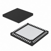
MAX9218ETM+ Maxim Integrated Products, MAX9218ETM+ Datasheet - Page 2

MAX9218ETM+
Manufacturer Part Number
MAX9218ETM+
Description
IC DESERIALIZER LVDS 48-TQFN
Manufacturer
Maxim Integrated Products
Datasheet
1.MAX9218ETMT.pdf
(15 pages)
Specifications of MAX9218ETM+
Function
Deserializer
Data Rate
700Mbps
Input Type
LVDS
Output Type
LVCMOS
Number Of Inputs
1
Number Of Outputs
27
Voltage - Supply
3 V ~ 3.6 V
Operating Temperature
-40°C ~ 85°C
Mounting Type
Surface Mount
Package / Case
48-TQFN Exposed Pad
Maximum Operating Temperature
+ 85 C
Minimum Operating Temperature
- 40 C
Mounting Style
SMD/SMT
Lead Free Status / RoHS Status
Lead free / RoHS Compliant
27-Bit, 3MHz-to-35MHz
DC-Balanced LVDS Deserializer
ABSOLUTE MAXIMUM RATINGS
V
Any Ground to Any Ground...................................-0.5V to +0.5V
IN+, IN- to LVDS GND...........................................-0.5V to +4.0V
IN+, IN- Short Circuit to LVDS GND or V
IN+, IN- Short Through 0.125µF (or smaller),
(R/F, OUTEN, RNG_, REFCLK,
(RGB_OUT[17:0], CNTL_OUT[8:0], DE_OUT, PCLK_OUT,
Continuous Power Dissipation (T
DC ELECTRICAL CHARACTERISTICS
(V
to V
T
Stresses beyond those listed under “Absolute Maximum Ratings” may cause permanent damage to the device. These are stress ratings only, and functional
operation of the device at these or any other conditions beyond those indicated in the operational sections of the specifications is not implied. Exposure to
absolute maximum rating conditions for extended periods may affect device reliability.
2
SINGLE-ENDED INPUTS (R/F, OUTEN, RNG0, RNG1, REFCLK, PWRDWN)
High-Level Input Voltage
Low-Level Input Voltage
Input Current
Input Clamp Voltage
SINGLE-ENDED OUTPUTS (RGB_OUT[17:0], CNTL_OUT[8:0], DE_OUT, PCLK_OUT, LOCK)
High-Level Output Voltage
Low-Level Output Voltage
High-Impedance Output Current
A
CC_
CC_
25V Series Capacitor..........................................-0.5V to +16V
PWRDWN) to GND .................................-0.5V to (V
LOCK) to V
48-Lead LQFP (derate 21.7mW/°C above +70°C) ....1739mW
48-Lead Thin QFN (derate 37mW/°C above +70°C) .2963mW
= +25°C.) (Notes 1, 2)
CC
_______________________________________________________________________________________
to _GND........................................................-0.5V to +4.0V
= +3.0V to +3.6V, PWRDWN = high, differential input voltage ⏐V
- ⏐V
PARAMETER
ID
CCO
/2⏐, T
GND ...........................-0.5V to (V
A
= -40°C to +85°C, unless otherwise noted. Typical values are at V
A
= +70°C)
SYMBOL
CCLVDS
V
V
V
V
I
V
I
OZ
OH
IN
CL
OL
IH
IL
......Continuous
V
PWRDWN = high or low
I
I
I
RNG1, RNG0 = high
I
simultaneously
I
I
RNG1, RNG0 = high
I
simultaneously
PWRDWN = low or OUTEN = low,
V
CL
OH
OH
OH
OL
OL
OL
IN
O
CCO
CC
= -0.3V to V
= -18mA
= 100µA
= 2mA,
= 2mA, RNG1, RNG0 both not high
= -0.3V to (V
= -100µA
= -2mA,
= -2mA, RNG1, RNG0 both not high
+ 0.5V)
+ 0.5V)
CONDITIONS
CCO
CC
ID
+ 0.3V),
ESD Protection
ISO 10605 (R
Storage Temperature Range .............................-65°C to +150°C
Junction Temperature ......................................................+150°C
Lead Temperature (soldering, 10s) .................................+300°C
+ 0.3V
⏐ = 0.05V to 1.2V, input common-mode voltage V
Machine Model (R
Human Body Model (R
Contact Discharge (IN+, IN-) to GND............................±10kV
Air Discharge (IN+, IN-) to GND ....................................±30kV
All Pins to GND ...........................................................±200V
All Pins to GND ..........................................................±3.0kV
D
= 2kΩ, C
D
CC_
= 0Ω, C
V
V
V
S
D
CCO
CCO
CCO
= +3.3V, ⏐V
= 330pF)
MIN
-0.3
2.0
-70
-10
= 1.5kΩ, C
- 0.1
- 0.35
- 0.4
S
= 200pF)
TYP
S
ID
= 100pF)
⏐ = 0.2V, V
V
CC
MAX
+0.8
0.35
+70
+10
-1.5
0.1
0.3
+ 0.3
CM
CM
= ⏐V
UNITS
= 1.2V,
µA
µA
V
V
V
V
V
ID
/2⏐


