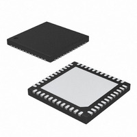
MAX9218ETM+ Maxim Integrated Products, MAX9218ETM+ Datasheet - Page 6

MAX9218ETM+
Manufacturer Part Number
MAX9218ETM+
Description
IC DESERIALIZER LVDS 48-TQFN
Manufacturer
Maxim Integrated Products
Datasheet
1.MAX9218ETMT.pdf
(15 pages)
Specifications of MAX9218ETM+
Function
Deserializer
Data Rate
700Mbps
Input Type
LVDS
Output Type
LVCMOS
Number Of Inputs
1
Number Of Outputs
27
Voltage - Supply
3 V ~ 3.6 V
Operating Temperature
-40°C ~ 85°C
Mounting Type
Surface Mount
Package / Case
48-TQFN Exposed Pad
Maximum Operating Temperature
+ 85 C
Minimum Operating Temperature
- 40 C
Mounting Style
SMD/SMT
Lead Free Status / RoHS Status
Lead free / RoHS Compliant
27-Bit, 3MHz-to-35MHz
DC-Balanced LVDS Deserializer
6
29–36,
25, 37
26, 38
15–23
39–48
PIN
10
11
12
13
14
24
27
28
—
_______________________________________________________________________________________
1
2
3
4
5
6
7
8
9
CNTL_OUT [8:0]
RGB_OUT [17:0]
V
PCLK_OUT
LVDS GND
PWRDWN
PLL GND
V
DE_OUT
CCO
REFCLK
V
OUTEN
NAME
CCLVDS
RNG1
RNG0
LOCK
V
GND
CCPLL
V
IN+
R/F
IN-
CCO
EP
CC
GND
Rising or Falling Latch Edge Select. LVTTL/LVCMOS input. Selects the edge of PCLK_OUT for
latching data into the next chip. Set R/F = high for a rising latch edge. Set R/F = low for a falling latch
edge. Internally pulled down to GND.
LVTTL/LVCMOS Range Select Input. Set to the range that includes the serializer parallel clock input
frequency. Internally pulled down to GND.
LVDS Supply Voltage. Bypass to LVDS GND with 0.1µF and 0.001µF capacitors in parallel as close
to the device as possible, with the smallest value capacitor closest to the supply pin.
Noninverting LVDS Serial Data Input
Inverting LVDS Serial Data Input
LVDS Supply Ground
PLL Supply Ground
PLL Supply Voltage. Bypass to PLL GND with 0.1µF and 0.001µF capacitors in parallel as close to
the device as possible, with the smallest value capacitor closest to the supply pin.
LVTTL/LVCMOS Range Select Input. Set to the range that includes the serializer parallel clock input
frequency. Internal pulldown to GND.
Digital Supply Ground
Digital Supply Voltage. Supply for LVTTL/LVCMOS inputs and digital circuits. Bypass to GND with
0.1µF and 0.001µF capacitors in parallel as close to the device as possible, with the smallest value
capacitor closest to the supply pin.
LVTTL/LVCMOS Reference Clock Input. Apply a reference clock that is within ±2% of the serializer
PCLK_IN frequency. Internally pulled down to GND.
LVTTL/LVCMOS Power-Down Input. Internally pulled down to GND.
LVTTL/LVCMOS Output Enable Input. High activates the single-ended outputs. Driving low places
the single-ended outputs in high impedance. Internally pulled down to GND.
LVTTL/LVCMOS Control Data Outputs. CNTL_OUT[8:0] are latched into the next chip on the rising or
falling edge of PCLK_OUT as selected by R/F when DE_OUT is low, and are held at the last state
when DE_OUT is high.
LVTTL/LVCMOS Data Enable Output. High indicates RGB_OUT[17:0] are active. Low indicates
CNTL_OUT[8:0] are active.
Output Supply Ground
Output Supply Voltage. Bypass to GND with 0.1µF and 0.001µF capacitors in parallel as close to the
device as possible, with the smallest value capacitor closest to the supply pin.
LVTTL/LVCMOS Lock Indicator Output. Outputs are valid when LOCK is low.
LVTTL/LVCMOS Parallel Clock Output. Latches data into the next chip on the edge selected by R/F.
LVTTL/LVCMOS Red, Green, and Blue Digital Video Data Outputs. RGB_OUT[17:0] are latched into
the next chip on the edge of PCLK_OUT selected by R/F when DE_OUT is high, and are held at the
last state when DE_OUT is low.
Exposed Pad for Thin QFN Package Only. Connect to GND.
FUNCTION
Pin Description


