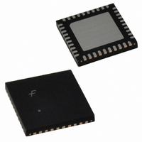
FIN24ACMLX Fairchild Semiconductor, FIN24ACMLX Datasheet - Page 8

FIN24ACMLX
Manufacturer Part Number
FIN24ACMLX
Description
IC SERIALIZER/DESERIALZR 40MLP
Manufacturer
Fairchild Semiconductor
Series
SerDes™r
Datasheet
1.FIN24ACMLX.pdf
(25 pages)
Specifications of FIN24ACMLX
Function
Serializer/Deserializer
Data Rate
520Mbps
Input Type
LVCMOS
Output Type
LVCMOS
Number Of Inputs
20
Number Of Outputs
20
Voltage - Supply
1.65 V ~ 3.6 V
Operating Temperature
-30°C ~ 70°C
Mounting Type
Surface Mount
Package / Case
40-MLP
Lead Free Status / RoHS Status
Lead free / RoHS Compliant
© 2005 Fairchild Semiconductor Corporation
FIN24AC Rev. 1.0.3
Deserializer Operation: DIRI = 0
Deserializer Operation: DIRI = 0
Deserializer Operation Mode
The operation of the deserializer is only dependent upon the data received on the DSI data signal pair and the CKSI
clock signal pair. The following two sections describe the operation of the deserializer under two distinct serializer
source conditions. References to the CKREF and STROBE signals refer to the signals associated with the serializer
device used in generating the serial data and clock signals that are inputs to the deserializer.
When operating in this mode, the internal serializer circuitry is disabled; including the parallel data input buffers. If there
is a CKREF signal provided, the CKSO serial clock continues to transmit bit clocks. Upon device power-up (S1 or S2 =
1), all deserializer output data pins are driven LOW until valid data is passed through the deserializer.
(Serializer Source:
CKREF = STROBE)
(Serializer Source:
CKREF does not = STROBE)
DP[1:24]
CKPO
DP[1:24]
CKSI
DSI
CKPO
CKSI
Figure 8. Deserializer Timing Diagram (Serializer Source: CKREF does not equal STROBE)
DSI
WORD n-2
b
Figure 7. Deserializer Timing Diagram (Serializer Source: CKREF equals STROBE)
WORD n-1
24
WORD n-2
b
WORD n-1
24
b
25
b
25
b
26
b
26
b
1
0
When the DIRI signal is asserted LOW, the device is configured as a deserializer.
Data is captured on the serial port and deserialized through use of the bit clock
sent with the data. The word boundary is defined in the actual clock and data sig-
nal. Parallel data is generated at the time the word boundary is detected. The fall-
ing edge of CKP occurs approximately six bit times after the falling edge of CKSI.
The rising edge of CKP goes high approximately 13 bit times after CKP goes
LOW. The rising edge of CKP is generated approximately 13 bit times later. When
no embedded word boundary occurs, no pulse is generated on CKP and CKP
remains HIGH.
The logical operation of the deserializer remains the same if the CKREF is equal
in frequency to the STROBE or at a higher frequency than the STROBE. The
actual serial data stream presented to the deserializer, however, differs because it
has non-valid data bits sent between words. The duty cycle of CKP varies based
on the ratio of the frequency of the CKREF signal to the STROBE signal. The fre-
quency of the CKP signal is equal to the STROBE frequency. The falling edge of
CKP will occurs six bit times after the data transition. The LOW time of the CKP
signal is equal to half (13 bit times) of the CKREF period. The CKP HIGH time is
equal to STROBE period – half of the CKREF period. Figure 8 is representative of
a waveform that could be seen when CKREF is not equal to STROBE. If CKREF
is significantly faster, additional non-valid data bits occur between data words.
0
6 bit times
b
6
b
7
b
j
b
b
8
j+1
WORD n-1
8
WORD n-1
13 bit times
b
WORD n
9
WORD n
b
b
j+13
19
b
b
j+14
20
b
24
b
24
b
25
b
25
b
26
b
26
WORD n
www.fairchildsemi.com
WORD n+1
WORD n
b
WORD n+1
1
0
b
2
0


