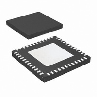
DS42MB200TSQ/NOPB National Semiconductor, DS42MB200TSQ/NOPB Datasheet

DS42MB200TSQ/NOPB
Specifications of DS42MB200TSQ/NOPB
Available stocks
Related parts for DS42MB200TSQ/NOPB
DS42MB200TSQ/NOPB Summary of contents
Page 1
... All receiver inputs are internally terminated with 100Ω differential terminating resistors. All driver outputs are inter- nally terminated with 50Ω Functional Block Diagram © 2009 National Semiconductor Corporation DS42MB200 Features ■ 1– 4.25 Gbps fully differential data paths ■ ...
Page 2
Simplified Block Diagram www.national.com 2 20178631 ...
Page 3
Connection Diagram Order number DS42MB200TSQ See NS Package Number SQA48D 3 20178632 www.national.com ...
Page 4
Pin Descriptions Pin Name Pin Number I/O LINE SIDE HIGH SPEED DIFFERENTIAL IO's LI_0 Inverting and non-inverting differential inputs of port_0 at the line side. LI_0+ and LI_0− have an LI_0− 7 internal 50Ω connected to an internal ...
Page 5
Pin Name Pin Number I/O POWER 14, 20 29, 35, 38, Each V 44 via located as close as possible to the landing pad of the recommended to have a ...
Page 6
Pre-Emphasis Level in PreL_[1:0] mV (VODB 1200 0 1 1200 1 0 1200 1 1 1200 (default) Pre-Emphasis Level in mV PreS_[1:0] (VODB 1200 0 1 1200 1 0 1200 1 1 1200 (default) FIGURE 1. ...
Page 7
... Absolute Maximum Ratings If Military/Aerospace specified devices are required, please contact the National Semiconductor Sales Office/ Distributors for availability and specifications. Supply Voltage ( CMOS/TTL Input Voltage CML Input/Output Voltage Junction Temperature Storage Temperature Lead Temperature Soldering, 4 sec Thermal Resistance, θ JA Thermal Resistance, θ ...
Page 8
Symbol Parameter V Output Pre-Emphasis R PE Voltage Ratio Running K28.7 pattern at 4.25 Gbps 20*log(VODPE/VODB) PREx_[1:0]=00 PREx_[1:0]=01 PREx_[1:0]=10 PREx_[1:0]=11 x=S for switch side pre-emphasis control x=L for line side pre-emphasis control See Figure 1 on waveform. See Figure 5 ...
Page 9
Symbol Parameter DJ Device Deterministic See Figure 5 for test circuit. Jitter (Notes 6, 8) Pre-emphasis disabled. At 4.25 Gbps, PRBS7 pattern for DS42MB200@ – 40° to 85°C DR Maximum Data Rate Tested with alternating-1-0 pattern MAX (Note 8) Note ...
Page 10
FIGURE 4. Test condition for output pre-emphasis duration FIGURE 6. Receiver Input Termination and Biasing Circuit www.national.com FIGURE 5. AC Test Circuit 20178650 10 20178639 20178634 ...
Page 11
Applications Information The DS42MB200 input equalizer provides equalization to compensate about transmission loss from a short backplane transmission line. For characterization purposes, a 25-inch FR4 coupled micro-strip board trace is used in place Finished Trace Trace Length ...
Page 12
FIGURE 8. Data input and output eye patterns with driver set to 9dB pre-emphasis www.national.com 12 20178643 ...
Page 13
FIGURE 9. Application diagram (showing data paths of port 0) 13 20178644 www.national.com ...
Page 14
Physical Dimensions www.national.com inches (millimeters) unless otherwise noted LLP-48 Package Order number DS42MB200TSQ See NS Package Number SQA48D 14 ...
Page 15
Notes 15 www.national.com ...
Page 16
... For more National Semiconductor product information and proven design tools, visit the following Web sites at: Products Amplifiers www.national.com/amplifiers Audio www.national.com/audio Clock and Timing www.national.com/timing Data Converters www.national.com/adc Interface www.national.com/interface LVDS www.national.com/lvds Power Management www.national.com/power Switching Regulators www.national.com/switchers LDOs www.national.com/ldo LED Lighting www ...


