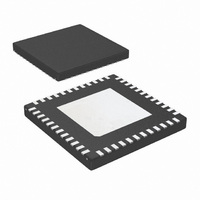
DS42MB200TSQ/NOPB National Semiconductor, DS42MB200TSQ/NOPB Datasheet - Page 8

DS42MB200TSQ/NOPB
Manufacturer Part Number
DS42MB200TSQ/NOPB
Description
IC MUX/BUFF DUAL 4.25GBPS 48-LLP
Manufacturer
National Semiconductor
Type
MUXr
Datasheet
1.DS42MB200TSQNOPB.pdf
(16 pages)
Specifications of DS42MB200TSQ/NOPB
Tx/rx Type
CML
Delay Time
2.0ns
Voltage - Supply
3.135 V ~ 3.465 V
Mounting Type
Surface Mount
Package / Case
48-LLP
Lead Free Status / RoHS Status
Lead free / RoHS Compliant
Current - Supply
-
Capacitance - Input
-
Other names
DS42MB200TSQTR
Available stocks
Company
Part Number
Manufacturer
Quantity
Price
Company:
Part Number:
DS42MB200TSQ/NOPB
Manufacturer:
Atmel
Quantity:
98
www.national.com
V
t
R
R
ΔR
V
POWER DISSIPATION
P
AC CHARACTERISTICS
t
t
t
t
t
t
t
t
RJ
PE
R
F
PLH
PHL
SKP
SKO
SKPP
SM
Symbol
PE
OCM
D
OTSE
OTD
OTSE
Output Pre-Emphasis
Voltage Ratio
20*log(VODPE/VODB)
Pre-Emphasis Width
(Note 8)
Output Termination
Output Differential
Termination
Mis-Match in Output
Termination Resistors
Output Common Mode
Voltage
Power Dissipation
Differential Low to High
Transition Time
Differential High to Low
Transition Time
Differential Low to High
Propagation Delay
Differential High to Low
Propagation Delay
Pulse Skew (Note 8)
Output Skew
(Notes 7, 8)
Part-to-Part Skew
(Note 8)
Mux Switch Time
Device Random Jitter
(Notes 5, 8)
Parameter
R
Running K28.7 pattern at 4.25 Gbps
PREx_[1:0]=00
PREx_[1:0]=01
PREx_[1:0]=10
PREx_[1:0]=11
x=S for switch side pre-emphasis control
x=L for line side pre-emphasis control
See Figure 1 on waveform.
See Figure 5 for test circuit.
Tested at −9 dB pre-emphasis level, PREx[1:0]=11
x=S for switch side pre-emphasis control
x=L for line side pre-emphasis control
See Figure 4 on measurement condition.
On-chip termination from OUT+ or OUT− to V
On-chip differential termination between OUT+ and
OUT−
Mis-match in output terminations at OUT+ and OUT
−
V
All outputs terminated by 100Ω ±1%.
PREL_[1:0]=0, PRES_[1:0]=0
Running PRBS 2
Measured with a clock-like pattern at 100 MHz,
between 20% and 80% of the differential output
voltage. Pre-emphasis disabled.
Transition time is measured with fixture as shown
in Figure 5, adjusted to reflect the transition time at
the output pins.
Measured at 50% differential voltage from input to
output.
|t
Difference in propagation delay among data paths
in the same device.
Difference in propagation delay between the same
output from devices operating under identical
condition.
Measured from V
loopback control to 50% of the valid differential
output.
See Figure 5 for test circuit.
Alternating-1-0 pattern.
Pre-emphasis disabled.
At 1.25 Gbps
At 4.25 Gbps
PHL
DD
L
= 100Ω ±1%
= 3.465V
–t
PLH
|
7
IH
-1 pattern at 4.25 Gbps
Conditions
or V
IL
of the mux-control or
8
CC
Min
125
2.4
42
(Note 2)
Typ
200
100
0.5
0.5
1.8
−3
−6
−9
50
80
80
0
Max
250
200
500
2.9
58
20
5
1
2
2
6
2
2
psrms
psrms
Units
dB
dB
dB
dB
ps
ps
ps
ns
ns
ps
ps
ps
ns
%
W
Ω
Ω
V


