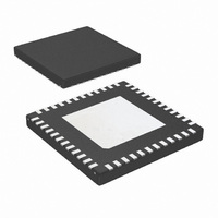
DS42MB200TSQ/NOPB National Semiconductor, DS42MB200TSQ/NOPB Datasheet - Page 5

DS42MB200TSQ/NOPB
Manufacturer Part Number
DS42MB200TSQ/NOPB
Description
IC MUX/BUFF DUAL 4.25GBPS 48-LLP
Manufacturer
National Semiconductor
Type
MUXr
Datasheet
1.DS42MB200TSQNOPB.pdf
(16 pages)
Specifications of DS42MB200TSQ/NOPB
Tx/rx Type
CML
Delay Time
2.0ns
Voltage - Supply
3.135 V ~ 3.465 V
Mounting Type
Surface Mount
Package / Case
48-LLP
Lead Free Status / RoHS Status
Lead free / RoHS Compliant
Current - Supply
-
Capacitance - Input
-
Other names
DS42MB200TSQTR
Available stocks
Company
Part Number
Manufacturer
Quantity
Price
Company:
Part Number:
DS42MB200TSQ/NOPB
Manufacturer:
Atmel
Quantity:
98
POWER
V
GND
GND
Pin Name
CC
Note: I = Input, O = Output, P = Power
Functional Description
The DS42MB200 is a signal conditioning 2:1 multiplexer and
a 1:2 buffer designed to support port redundancy up to 4.25
Gbps. Each input stage has a fixed equalizer that provides
equalization to compensate about 5 dB of transmission loss
from a short backplane trace (about 10 inches backplane).
The output driver has pre-emphasis (driver-side equalization)
to compensate the transmission loss of the backplane that it
is driving. The driver conditions the output signal such that the
lower frequency and higher frequency pulses reach approxi-
mately the same amplitude at the end of the backplane, and
minimize the deterministic jitter caused by the amplitude dis-
parity. The DS42MB200 provides 4 steps of user-selectable
pre-emphasis ranging from 0, -3, -6 and –9 dB to handle dif-
ferent lengths of backplane. Figure 1 shows a driver pre-
emphasis waveform. The pre-emphasis duration is 200ps
nominal, corresponds to 0.8 bit-width at 4 Gbps. The pre-em-
5, 11, 17, 32,
Pin Number
2, 8, 14, 20,
29, 35, 38,
DAP
44
41
MUX_S0
0
1 (default)
MUX_S1
0
1 (default)
LB0A
0
1 (default)
LB0B
0
1 (default)
LB1A
0
1 (default)
LB1B
0
1 (default)
I/O
P
P
P
V
Each V
via located as close as possible to the landing pad of the V
It is recommended to have a 0.01 μF or 0.1 μF, X7R, size-0402 bypass capacitor from each V
pin to ground plane.
Ground reference. Each ground pin should be connected to the ground plane through a low
inductance path, typically with a via located as close as possible to the landing pad of the GND pin.
Die Attach Pad (DAP) is the metal contact at the bottom side, located at the center of the LLP-48
package. It should be connected to the GND plane with at least 4 via to lower the ground impedance
and improve the thermal performance of the package.
CC
TABLE 1. LOGIC TABLE FOR MULTIPLEX CONTROLS
TABLE 2. LOGIC TABLE FOR LOOPBACK Controls
= 3.3V ± 5%.
CC
Mux Function
MUX_0 select switch_B input, SIB_0±.
MUX_0 select switch_A input, SIA_0±.
Mux Function
MUX_1 select switch_B input, SIB_1±.
MUX_1 select switch_A input, SIA_0±.
Loopback Function
Enable loopback from SIA_0± to SOA_0±.
Normal mode. Loopback disabled.
Loopback Function
Enable loopback from SIB_0± to SOB_0±.
Normal mode. Loopback disabled.
Loopback Function
Enable loopback from SIA_1± to SOA_1±.
Normal mode. Loopback disabled.
Loopback Function
Enable loopback from SIB_1± to SOB_1±.
Normal mode. Loopback disabled.
pin should be connected to the V
5
phasis levels of switch-side and line-side can be individually
programmed.
The high speed inputs are self-biased to about 1.5V and are
designed for AC coupling allowing the DS42MB200 to be di-
rectly inserted into the datapath without any limitation. The
ideal AC coupling capacitor value is often based on the lowest
frequency component embedded within the serial link. A typ-
ical AC coupling capacitor value ranges between 100 and
1000nF, some specifications with scrambled data may re-
quire a larger coupling capacitor for optimal performance. To
reduce unwanted parasitics around and within the AC cou-
pling capacitor, a body size of 0402 is recommended. Figure
5 shows the AC coupling capacitor placement in an AC test
circuit. The inputs are compatible to most AC coupling differ-
ential signals such as LVDS, LVPECL and CML. See Figure
6 for details.
Description
CC
plane through a low inductance path, typically with a
CC
pin.
www.national.com
CC


