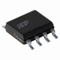
P82B96TD,112 NXP Semiconductors, P82B96TD,112 Datasheet - Page 18

P82B96TD,112
Manufacturer Part Number
P82B96TD,112
Description
IC I2C BUS BUFFER DUAL 8-SOIC
Manufacturer
NXP Semiconductors
Type
Bufferr
Datasheet
1.P82B96TD118.pdf
(32 pages)
Specifications of P82B96TD,112
Package / Case
8-SOIC (3.9mm Width)
Tx/rx Type
I²C Logic
Delay Time
5.0ns
Capacitance - Input
7pF
Voltage - Supply
2 V ~ 15 V
Current - Supply
900µA
Mounting Type
Surface Mount
Logic Family
P82B
Supply Voltage (max)
15 V
Supply Voltage (min)
2 V
Maximum Operating Temperature
85 C
Mounting Style
SMD/SMT
Maximum Power Dissipation
300 mW
Minimum Operating Temperature
- 40 C
Number Of Lines (input / Output)
4 / 2
Propagation Delay Time
90 ns
Logic Type
Bus Buffer
Lead Free Status / RoHS Status
Lead free / RoHS Compliant
For Use With
OM6285 - EVAL BOARD I2C-2002-1A568-4002 - DEMO BOARD I2C
Lead Free Status / Rohs Status
Lead free / RoHS Compliant
Other names
568-3982-5
935262295112
P82B96TD
P82B96TD
935262295112
P82B96TD
P82B96TD
NXP Semiconductors
P82B96_8
Product data sheet
Fig 19. Propagation Sx to Tx (Sx pull-up to 5 V;
V
14
10
6
2
2
0
Frequency = 624 kHz
Tx pull-up to V
10.2 Negative undershoot below absolute minimum value
400
Tx
Sx
The reason why the IC pin reverse voltage on pins Tx and Rx in
is specified at such a low value, 0.3 V, is not that applying larger voltages is likely to
cause damage but that it is expected that, in normal applications, there is no reason why
larger DC voltages will be applied. This ‘absolute maximum’ specification is intended to be
a DC or continuous ratings and the nominal DC I
even reach 0 V. Inside P82B96 at every pin there is a large protective diode connected to
the GND pin and that diode will start to conduct when the pin voltage is more than about
Figure 21
plot was made using a curve tracer that applies 50 Hz mains voltage via a series resistor,
so the pulse durations are long duration (several milliseconds) and are reaching peaks of
over 2 A when more than 1.5 V is applied. The IC becomes very hot during this testing
but it was not damaged. Whenever there is current flowing in any of these diodes it is
possible that there can be faulty operation of any IC. For that reason we put a specification
on the negative voltage that is allowed to be applied. It is selected so that, at the highest
allowed junction temperature, there will be a big safety factor that guarantees the diode
will not conduct and then we do not need to make any 100 % production tests to
guarantee the published specification.
For the P82B96, in specific applications, there will always be transient overshoot and
ringing on the wiring that can cause these diodes to conduct. Therefore we designed the
IC to withstand those transients and as a part of the qualification procedure we made
tests, using DC currents to more than twice the normal bus sink currents, to be sure that
the IC was not affected by those currents. For example, the Tx/Ty and Rx/Ry pins were
tested to at least 80 mA which, from
functioning of the P82B96 is not affected even by those large currents. The Absolute
Maximum (DC) ratings are not intended to apply to transients but to steady state
conditions. This explains why you will never see any problems in practice even if, during
transients, more than 0.3 V is applied to the bus interface pins of P82B96.
800
CC
0.55 V with respect to GND at 25 C ambient.
= 10 V)
1200
shows the measured characteristic for one of those diodes inside P82B96. The
1600
002aab995
ns
Rev. 08 — 10 November 2009
2000
Fig 20. Propagation Rx to Sx (Sx pull-up to 5 V;
Figure
V
14
10
6
2
2
0
Ch1 frequency = 624 kHz
Rx pull-up to V
21, would be more than 0.8 V. The correct
2
400
C-bus voltage LOW usually does not
Rx
Sx
800
CC
Dual bidirectional bus buffer
= 10 V)
1200
Table 4 “Limiting values”
1600
© NXP B.V. 2009. All rights reserved.
002aab996
P82B96
ns
2000
18 of 32


