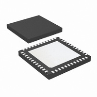
DS15MB200TSQX/NOPB National Semiconductor, DS15MB200TSQX/NOPB Datasheet

DS15MB200TSQX/NOPB
Specifications of DS15MB200TSQX/NOPB
Available stocks
Related parts for DS15MB200TSQX/NOPB
DS15MB200TSQX/NOPB Summary of contents
Page 1
... The 3.3V supply, CMOS process, and robust I/O ensure high performance at low power over the entire industrial -40 to +85˚C temperature range. Typical Application Block Diagram © 2006 National Semiconductor Corporation Features n 1.5 Gbps data rate per channel n Configurable off/on pre-emphasis drives lossy backplanes and cables ...
Page 2
Pin Descriptions Pin LLP Pin I/O, Type Name Number SWITCH SIDE DIFFERENTIAL INPUTS SIA_0 LVDS Switch A-side Channel 0 inverting and non-inverting differential inputs. LVDS, Bus LVDS, SIA_0− 29 CML, or LVPECL compatible. SIA_1 LVDS Switch ...
Page 3
Pin Descriptions (Continued) Pin LLP Pin I/O, Type Name Number POWER 12, I, Power 37, 43, 46, 48 GND Power Ground reference for LVDS and CMOS circuitry. (Note 2) For the ...
Page 4
Output Characteristics The output characteristics of the DS15MB200 have been optimized for point-to-point backplane and cable applica- tions, and are not intended for multipoint or multidrop signal- ing. A 100Ω output (source) termination resistor is incorporated in the device to ...
Page 5
Absolute Maximum Ratings Supply Voltage ( CMOS Input Voltage LVDS Receiver Input Voltage (Note 7) LVDS Driver Output Voltage LVDS Output Short Circuit Current Junction Temperature Storage Temperature Lead Temperature (Solder, 4sec) @ Max Pkg Power Capacity 25˚C ...
Page 6
Electrical Characteristics Over recommended operating supply and temperature ranges unless other specified. Symbol Parameter SUPPLY CURRENT (Static) I Supply Current CC I Supply Current - Powerdown CCZ Mode SWITCHING CHARACTERISTICS — LVDS OUTPUTS t Differential Low to High Transition LHT ...
Page 7
Typical Performance Characteristics Power Supply Current vs. Bit Data Rate Dynamic power supply current was measured with all channels active and toggling at the bit data rate. Data pattern has no effect on the power consumption 3.3V, T ...
Page 8
TRI-STATE and Powerdown Modes The DS15MB200 has output enable control on each of the six onboard LVDS output drivers. This control allows each output individually to be placed in a low power TRI-STATE mode while the device remains active, and ...
Page 9
Interfacing LVDS to LVPECL An LVDS driver consists of a current source (nominal 3.5mA) which drives a CMOS differential pair. It needs a differential resistive load in the range 130 ohms to generate LVDS levels ...
Page 10
... BANNED SUBSTANCE COMPLIANCE National Semiconductor manufactures products and uses packing materials that meet the provisions of the Customer Products Stewardship Specification (CSP-9-111C2) and the Banned Substances and Materials of Interest Specification (CSP-9-111S2) and contain no ‘‘Banned Substances’’ as defined in CSP-9-111S2. ...


