DS15MB200TSQX/NOPB National Semiconductor, DS15MB200TSQX/NOPB Datasheet - Page 9
DS15MB200TSQX/NOPB
Manufacturer Part Number
DS15MB200TSQX/NOPB
Description
IC MUX/BUFFER DUAL 1.5GBPS 48LLP
Manufacturer
National Semiconductor
Type
MUXr
Datasheet
1.DS15MB200TSQNOPB.pdf
(10 pages)
Specifications of DS15MB200TSQX/NOPB
Tx/rx Type
LVDS
Delay Time
1.0ns
Capacitance - Input
2pF
Voltage - Supply
3 V ~ 3.6 V
Current - Supply
275mA
Mounting Type
Surface Mount
Package / Case
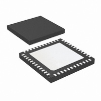
48-LLP
Lead Free Status / RoHS Status
Lead free / RoHS Compliant
Other names
DS15MB200TSQX
Available stocks
Company
Part Number
Manufacturer
Quantity
Price
Company:

Part Number:
DS15MB200TSQX/NOPB
Manufacturer:
TI/NS
Quantity:
260


Interfacing LVDS to LVPECL
An LVDS driver consists of a current source (nominal 3.5mA)
which drives a CMOS differential pair. It needs a differential
resistive load in the range of 70 to 130 ohms to generate
LVDS levels. In a system, the load should be selected to
match transmission line characteristic differential impedance
so that the line is properly terminated. The termination resis-
tor should be placed as close to the receiver inputs as
possible. When interfacing an LVDS driver with a non-LVDS
receiver, one only needs to bias the LVDS signal so that it is
within the common mode range of the receiver. This may be
done by using separate biasing voltage which demands
another power supply. Some receivers have required biasing
voltage available on-chip (V
Figure 4 illustrates interface between an LVDS driver and a
LVPECL with a V
the receiver (Note 16), provide proper resistive load for the
driver and termination for the transmission line, and V
desired bias for the receiver.
Figure 5 illustrates AC coupled interface between an LVDS
driver and LVPECL receiver without a V
resistors R1, R2, R3, and R4, if not present in the receiver
(Note 16), provide a load for the driver, terminate the trans-
mission line, and bias the signal for the receiver.
Note 16: The bias networks shown above for LVPECL drivers and receivers
may or may not be present within the driver device. The LVPECL driver and
receiver specification must be reviewed closely to ensure compatibility be-
tween the driver and receiver terminations and common mode operating
ranges.
FIGURE 4. DC Coupled LVDS to LVPECL Interface
FIGURE 5. AC Coupled LVDS to LVPECL Interface
T
pin available. R1 and R2, if not present in
T
, V
TT
or V
BB
T
).
pin available. The
20157364
20157363
T
sets
9
Packaging Information
The Leadless Leadframe Package (LLP) is a leadframe
based chip scale package (CSP) that may enhance chip
speed, reduce thermal impedance, and reduce the printed
circuit board area required for mounting. The small size and
very low profile make this package ideal for high density
PCBs used in small-scale electronic applications such as
cellular phones, pagers, and handheld PDAs. The LLP pack-
age is offered in the no Pullback configuration. In the no
Pullback configuration the standard solder pads extend and
terminate at the edge of the package. This feature offers a
visible solder fillet after board mounting.
The LLP has the following advantages:
For more details about LLP packaging technology, refer to
applications note AN-1187, "Leadless Leadframe Package"
• Low thermal resistance
• Reduced electrical parasitics
• Improved board space efficiency
• Reduced package height
•
Reduced package mass
www.national.com
Related parts for DS15MB200TSQX/NOPB
Image
Part Number
Description
Manufacturer
Datasheet
Request
R

Part Number:
Description:
National Semiconductor [8-Bit D/A Converter]
Manufacturer:
National Semiconductor
Datasheet:
Part Number:
Description:
National Semiconductor [Media Coprocessor]
Manufacturer:
National Semiconductor
Datasheet:
Part Number:
Description:
Digitally Controlled Tone and Volume Circuit with Stereo Audio Power Amplifier, Microphone Preamp Stage and National 3D Sound
Manufacturer:
National Semiconductor
Datasheet:
Part Number:
Description:
Digitally Controlled Tone and Volume Circuit with Stereo Audio Power Amplifier, Microphone Preamp Stage and National 3D Sound
Manufacturer:
National Semiconductor
Datasheet:
Part Number:
Description:
AC97 Rev 2 Codec with Sample Rate Conversion and National 3D Sound
Manufacturer:
National Semiconductor
Part Number:
Description:
Manufacturer:
National Semiconductor
Datasheet:
Part Number:
Description:
Manufacturer:
National Semiconductor
Datasheet:
Part Number:
Description:
General Purpose, Low Voltage, Low Power, Rail-to-Rail Output Operational Amplifiers
Manufacturer:
National Semiconductor
Datasheet:
Part Number:
Description:
8-bit 20 MSPS flash A/D converter.
Manufacturer:
National Semiconductor
Datasheet:
Part Number:
Description:
Low Noise Quad Operational Amplifier
Manufacturer:
National Semiconductor
Datasheet:
Part Number:
Description:
Quad Differential Line Receivers
Manufacturer:
National Semiconductor
Datasheet:
Part Number:
Description:
Quad High Speed Trapezoidal? Bus Transceiver
Manufacturer:
National Semiconductor
Datasheet:
Part Number:
Description:
Dual Line Receiver
Manufacturer:
National Semiconductor
Datasheet:
Part Number:
Description:
TTL to 10k ECL Level Translator with Latch
Manufacturer:
National Semiconductor
Datasheet: