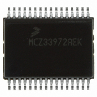
MCZ33972AEK Freescale Semiconductor, MCZ33972AEK Datasheet - Page 14

MCZ33972AEK
Manufacturer Part Number
MCZ33972AEK
Description
IC MULTIPLE SWITCH DETECT 32SOIC
Manufacturer
Freescale Semiconductor
Datasheet
1.MCZ33972AEK.pdf
(32 pages)
Specifications of MCZ33972AEK
Applications
Switch Monitoring
Interface
SPI
Voltage - Supply
8 V ~ 26 V
Package / Case
32-SOIC (7.5mm Width) Exposed Pad, 32-eSOIC, 32-HSOIC
Mounting Type
Surface Mount
Lead Free Status / RoHS Status
Lead free / RoHS Compliant
Available stocks
Company
Part Number
Manufacturer
Quantity
Price
Part Number:
MCZ33972AEK
Manufacturer:
FREESCALE
Quantity:
20 000
Part Number:
MCZ33972AEKR2
Manufacturer:
FREESCALE
Quantity:
20 000
POWER SUPPLY
VPWR pin. Characteristics are provided from 8.0 to 16 V for
the device. Switch contact currents and the internal logic
supply are generated from the VPWR pin. The VDD supply
pin is used to set the SPI communication voltage levels,
current source for the SO driver, and pull-up current on
and
reduce quiescent current. If V
is in Normal mode, the device will remain in Normal mode. If
V
Sleep mode until a wake-up input is received (
LOW, switch input or interrupt timer expires).
communication and will not allow the device to wake up from
INT
POWER-ON RESET (POR)
and place the device in Normal mode.
Reset Command are as follows:
NORMAL AND SLEEP MODES
Sleep mode. A discussion on Normal mode begins below.
A discussion on Sleep mode begins on page 19.
Normal Mode
Table 6. Settings Command
WAKE-UP / INTERRUPT REGISTER
allowed to wake the 33972 from Sleep Mode or set the
pin LOW in Normal mode. Programming the wake-up /
generating an interrupt and will disable the specific input from
14
interrupt bit to logic [0] will disable the specific input from
33972
FUNCTIONAL DEVICE OPERATION
OPERATIONAL MODES
DD
23
0
The 33972 is designed to operate from 5.5 to 40 V on the
The VDD supply may be removed from the device to
Removing V
Applying V
Default settings from Power-ON Reset via V
• Programmable switch – set to switch to battery
• All inputs set as wake-up
• Wetting current on (16 mA)
• Wetting current timer on (20 ms)
• All inputs tri-state
• Analog select 00000 (no input channel selected)
The 33972 has two operating modes, Normal mode and
Normal mode may be entered by the following events:
• Application of V
• Change-of-switch state (when enabled)
The wake-up / interrupt register defines the inputs that are
and
CS
is removed in Sleep mode, the device will remain in
22
.
0
CS
pins.
Settings Command
21
0
PWR
DD
20
to the device will cause a Power-ON Reset
0
from the device disables SPI
PWR
19
0
to the IC
18
0
DD
is removed while the device
17
0
16
1
15
X
WAKE
PWR
14
X
or the
HIGH to
13
X
INT
INT
Not used
12
X
11
X
the 33972 be programmed through the SPI.
are listed below. Further explanation of each register is
provided in subsequent paragraphs.
operation in Normal mode. Switch states are latched into the
input register on the falling edge of
is cleared on the rising edge of CS. However,
clear on rising edge of
communication (
being missed by the MCU.
PROGRAMMABLE SWITCH REGISTER
battery or switch-to-ground. These inputs types are defined
using the settings command
for switch-to-battery, a logic [1] for the appropriate bit must be
set. To set an SPn input for switch-to-ground, a logic [0] for
the appropriate bit must be set. The MCU may change or
update the programmable switch register via software at any
time in Normal mode. Regardless of the setting, when the
SPn input switch is closed a logic [1] will be placed in the
serial output response register
waking the IC in Sleep mode
wake-up /interrupt bit to logic [1] will enable the specific input
to generate an interrupt with switch change of state and will
enable the specific input as wake-up. The MCU may change
or update the wake-up / interrupt register via software at any
time in Normal mode.
• Falling edge of
• Falling edge of
• Falling edge of
• Interrupt timer expires
Only in Normal mode with V
The registers that may be programmed in Normal mode
•Programmable Switch Register
•Wake-Up / Interrupt Register
•Wetting Current Register
•Wetting Current Timer Register
•Tri-State Register
•Analog Select Register
•Calibration of Timers
•Reset
Figure
Inputs SP0 to SP7 may be programmable for switch-to-
10
X
Logic [1])
Command )
Enable Command )
X
9
6, page 9, is a graphical description of the device
(Reset Command )
X
8
CS
sp7 sp6 sp5 sp4 sp3 sp2 sp1 sp0
LOW). This prevents switch states from
7
WAKE
INT
CS
(Tri-state Command )
Analog Integrated Circuit Device Data
CS
(with V
(with V
(Calibration Command )
6
if a switch has closed during SPI
(Analog Command )
Battery/Ground Select
(Table
(Metallic Command )
(Table
DD
5
(Table
DD
DD
(Wake-up / Interrupt
applied can the registers of
= 5.0 V)
Freescale Semiconductor
= 5.0 V and
(Settings Command )
CS
(Wetting Current Timer
6). To set an SPn input
4
7). Programming the
17, page 19).
. The
3
INT
INT
2
WAKE
to the MCU
will not
1
at
0


