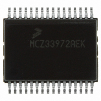
MCZ33972AEK Freescale Semiconductor, MCZ33972AEK Datasheet - Page 8

MCZ33972AEK
Manufacturer Part Number
MCZ33972AEK
Description
IC MULTIPLE SWITCH DETECT 32SOIC
Manufacturer
Freescale Semiconductor
Datasheet
1.MCZ33972AEK.pdf
(32 pages)
Specifications of MCZ33972AEK
Applications
Switch Monitoring
Interface
SPI
Voltage - Supply
8 V ~ 26 V
Package / Case
32-SOIC (7.5mm Width) Exposed Pad, 32-eSOIC, 32-HSOIC
Mounting Type
Surface Mount
Lead Free Status / RoHS Status
Lead free / RoHS Compliant
Available stocks
Company
Part Number
Manufacturer
Quantity
Price
Part Number:
MCZ33972AEK
Manufacturer:
FREESCALE
Quantity:
20 000
Part Number:
MCZ33972AEKR2
Manufacturer:
FREESCALE
Quantity:
20 000
Table 5. Dynamic Electrical Characteristics
noted. Where applicable, typical values reflect the parameter’s approximate average value with V
8
SWITCH INPUT
DIGITAL INTERFACE TIMING
Notes
33972
ELECTRICAL CHARACTERISTICS
DYNAMIC ELECTRICAL CHARACTERISTICS
Pulse Wetting Current Time
Interrupt Delay Time
Sleep Mode Switch Scan Time
Calibrated Scan Timer Accuracy
Calibrated Interrupt Timer Accuracy
Required Low-state Duration on V
Falling Edge of CS to Rising Edge of SCLK
Falling Edge of SCLK to Rising Edge of
SI to Falling Edge of SCLK
Falling Edge of SCLK to SI
SI,
SI,
Time from Falling Edge of
Time from Rising Edge of
Time from Rising Edge of SCLK to SO Data Valid
13.
14.
15.
16.
17.
18.
Characteristics noted under conditions 3.1 V ≤ V
Normal Mode
Sleep Mode
Sleep Mode
V
Required Setup Time
Required Setup Time
Required Setup Time
Required Hold Time
CS
CS
PWR
, SCLK Signal Rise Time
, SCLK Signal Fall Time
These parameters are guaranteed by design. Production test equipment uses 4.16 MHz, 5.0 V SPI interface.
This parameter is guaranteed by design but not production tested.
Rise and Fall time of incoming SI,
Time required for valid output status data to be available on SO pin.
Time required for output states data to be terminated at SO pin.
Time required to obtain valid data out from SO following the rise of SCLK with 200 pF load.
≤ 0.2 V
CS
CS
to SO High-impedance
to SO Low-impedance
(13)
(15)
Characteristic
(15)
PWR
for Reset
CS
CS
DYNAMIC ELECTRICAL CHARACTERISTICS
, and SCLK signals suggested for design consideration to prevent the occurrence of double pulsing.
(14)
(18)
(16)
(17)
DD
≤ 5.25 V, 8.0 V ≤ V
t
t
SCAN TIMER
t
PULSE (ON)
t
PWR
INT TIMER
Symbol
t
t
SI (HOLD)
t
t
t
INT-DLY
SO (DIS)
t
SO (EN)
t
t
RESET
t
SI (SU)
t
VALID
SCAN
t
LEAD
R (SI)
F (SI)
LAG
≤ 16 V, -40°C ≤ T
Min
100
100
15
50
16
20
–
–
–
–
–
–
–
–
–
Analog Integrated Circuit Device Data
C
≤ 125°C, unless otherwise
PWR
Typ
200
5.0
5.0
5.0
16
25
–
–
–
–
–
–
–
–
–
Freescale Semiconductor
= 13 V, T
Max
300
20
16
10
10
10
55
55
55
–
–
–
–
–
–
A
= 25°C.
Unit
ms
μs
μs
μs
ns
ns
ns
ns
ns
ns
ns
ns
ns
%
%


