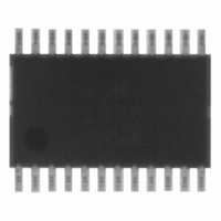
ADM1024ARUZ ON Semiconductor, ADM1024ARUZ Datasheet - Page 11

ADM1024ARUZ
Manufacturer Part Number
ADM1024ARUZ
Description
IC MONITOR SYS TEMP/VOLT 24TSSOP
Manufacturer
ON Semiconductor
Datasheet
1.ADM1024ARUZ.pdf
(29 pages)
Specifications of ADM1024ARUZ
Applications
PC's, PDA's
Interface
Serial
Voltage - Supply
2.8 V ~ 5.5 V
Package / Case
24-TSSOP
Mounting Type
Surface Mount
Temperature Sensor Function
Temp Sensor
Output Type
Digital
Package Type
TSSOP
Operating Temperature (min)
0C
Operating Temperature (max)
100C
Operating Temperature Classification
Commercial
Operating Supply Voltage (typ)
3.3V
Operating Supply Voltage (max)
5.5V
Full Temp Accuracy
+/- 2 C , +/- 3 C
Digital Output - Bus Interface
SMBus
Digital Output - Number Of Bits
10 bit
Supply Voltage (max)
12 V
Supply Voltage (min)
2.5 V
Maximum Operating Temperature
+ 100 C
Minimum Operating Temperature
0 C
Supply Current
1.4 mA
Lead Free Status / RoHS Status
Lead free / RoHS Compliant
Available stocks
Company
Part Number
Manufacturer
Quantity
Price
Part Number:
ADM1024ARUZ
Manufacturer:
ADI/亚德诺
Quantity:
20 000
Pins 22 to 24 when they are configured as interrupt inputs by
setting Bit 7 of the Channel Mode Register. This function is
controlled for Pins 20 and 21 by Bits 6 and 7 of Configuration
Register 2.
for external temperature−sensing diodes by programming Bit 2
of the Channel Mode Register.
core voltage ID bits (VID0 to VID4, Pins 24 to 20) to be
reconfigured as interrupt inputs.
Table 2.
A−to−D Converter
approximation, Analog−to−Digital Converter (ADC). This
has a resolution of eight bits. The basic input range is 0 V to
2.5 V, which is the input range of AIN1 and AIN2, but five
Table 3. A/D Output Code vs. V
12.000–12.063
15.312–15.375
15.375–15.437
15.437–15.500
15.500–15.563
15.563–15.625
15.625–15.688
15.688–15.750
15.750–15.812
15.812–15.875
Bits 4 to 6 of the Channel Mode Register enable or disable
Pins 17 and 18 can be configured as analog inputs or as inputs
Bit 7 of the Channel Mode Register allows the processor
A truth table for the Channel Mode Register is given in
These inputs are multiplexed into the on−chip, successive
0.062–0.125
0.125–0.188
0.188–0.250
0.250–0.313
0.313–0.375
0.375–0.438
0.438–0.500
0.500–0.563
4.000–4.063
8.000–8.063
+12 V
<0.062
IN
0.026–0.052
0.052–0.078
0.078–0.104
0.104–0.130
0.130–0.156
0.156–0.182
0.182–0.208
0.208–0.234
1.666–1.692
3.330–3.560
5.000–5.026
6.380–6.406
6.406–6.432
6.432–6.458
6.458–6.484
6.484–6.510
6.510–6.536
6.536–6.562
6.562–6.588
6.588–6.615
+5.0 V
<0.026
IN
V
0.017–0.034
0.034–0.052
0.052–0.069
0.069–0.086
0.086–0.103
0.103–0.120
0.120–0.138
0.138–0.155
1.100–1.117
2.200–2.217
3.300–3.317
4.210–4.230
4.230–4.245
4.245–4.263
4.263–4.280
4.280–4.300
4.300–4.314
4.314–4.331
4.331–4.348
4.348–4.366
CC
<0.0172
IN
(3.3 V)
Input Voltage
V
0.026–0.052
0.052–0.078
0.078–0.104
0.104–0.130
0.130–0.156
0.156–0.182
0.182–0.208
0.208–0.234
1.666–1.692
3.330–3.560
5.000–5.026
6.380–6.406
6.406–6.432
6.432–6.458
6.458–6.484
6.484–6.510
6.510–6.536
6.536–6.562
6.562–6.588
6.588–6.615
CC
<0.026
(5.0 V)
http://onsemi.com
0.013–0.026
0.026–0.039
0.039–0.052
0.052–0.065
0.065–0.078
0.078–0.091
0.091–0.104
0.833–0.846
1.667–1.680
2.500–2.513
3.190–3.203
3.203–3.216
3.216–3.229
3.229–3.242
3.242–3.255
3.255–3.268
3.268–3.281
3.281–3.294
3.294–3.307
0.104–0.117
+2.5 V
<0.013
11
−
−
−
−
−
−
−
−
−
−
−
−
IN
of the inputs have built−in attenuators to allow measurement
of 2.5 V, 5.0 V, 12 V, and the processor core voltages V
and V
the tolerance of these supply voltages, the ADC produces an
output of 3/4 full scale (decimal 192) for the nominal input
Table 2. Channel Mode Register
1. Power−On Default = 0000 0000
Register Bit
Channel
Mode
0.014–0.028
0.028–0.042
0.042–0.056
0.056–0.070
0.070–0.084
0.084–0.098
0.098–0.112
0.112–0.126
0.900–0.914
1.800–1.814
2.700–2.714
3.445–3.459
3.459–3.473
3.473–3.487
3.487–3.501
3.501–3.515
3.515–3.529
3.529–3.543
3.543–3.558
3.558–3.572
CCP2
0
1
2
3
4
5
6
7
+V
<0.014
CCP 1/2
without any external components. To allow for
Controls
Int. V
Pin(s)
17, 18
Meas.
20–24
0.010–0.019
0.019–0.029
0.029–0.039
0.039–0.049
0.049–0.058
0.058–0.068
0.068–0.078
0.078–0.087
0.625–0.635
1.250–1.260
1.875–1.885
2.392–2.402
2.402–2.412
2.412–2.422
2.422–2.431
2.431–2.441
2.441–2.451
2.451–2.460
2.460–2.470
2.470–2.480
24
23
22
5
6
A
<0.010
CC
IN (1/2)
0 = FAN1, 1 = A
0 = FAN2, 1 = A
0 = 2.5 V, V
0 = 3.3 V, 1 = 5.0 V
0 = VID0, 1 = IRQ0
0 = VID1, 1 = IRQ1
0 = VID2, 1 = IRQ2
0 = VID0 to VID4,
1 = Interrupt Inputs
(1/4−Scale)
(1/2−Scale)
(3/4−Scale)
Decimal
(Note 1)
128
192
245
246
247
248
249
250
251
252
253
64
0
1
2
3
4
5
6
7
8
Function
CCP2
A/D Output
IN1
IN2
, 1 = D2–, D2+
00000000
00000001
00000010
00000011
00000100
00000101
00000110
00000111
00001000
01000000
10000000
11000000
11110101
11110110
11111000
11111001
11111010
11110111
11111011
11111100
11111101
Binary
CCP1


