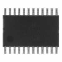
ADM1024ARUZ ON Semiconductor, ADM1024ARUZ Datasheet - Page 22

ADM1024ARUZ
Manufacturer Part Number
ADM1024ARUZ
Description
IC MONITOR SYS TEMP/VOLT 24TSSOP
Manufacturer
ON Semiconductor
Datasheet
1.ADM1024ARUZ.pdf
(29 pages)
Specifications of ADM1024ARUZ
Applications
PC's, PDA's
Interface
Serial
Voltage - Supply
2.8 V ~ 5.5 V
Package / Case
24-TSSOP
Mounting Type
Surface Mount
Temperature Sensor Function
Temp Sensor
Output Type
Digital
Package Type
TSSOP
Operating Temperature (min)
0C
Operating Temperature (max)
100C
Operating Temperature Classification
Commercial
Operating Supply Voltage (typ)
3.3V
Operating Supply Voltage (max)
5.5V
Full Temp Accuracy
+/- 2 C , +/- 3 C
Digital Output - Bus Interface
SMBus
Digital Output - Number Of Bits
10 bit
Supply Voltage (max)
12 V
Supply Voltage (min)
2.5 V
Maximum Operating Temperature
+ 100 C
Minimum Operating Temperature
0 C
Supply Current
1.4 mA
Lead Free Status / RoHS Status
Lead free / RoHS Compliant
Available stocks
Company
Part Number
Manufacturer
Quantity
Price
Part Number:
ADM1024ARUZ
Manufacturer:
ADI/亚德诺
Quantity:
20 000
RESET Input/Output
open−drain output, providing a low going 20 ms output pulse
when Bit 4 of the Configuration Register is set to 1, provided
the reset function has first been enabled by setting Bit 7 of
Interrupt Mask Registers 2 to 1. The bit is automatically
cleared when the reset pulse is output. Pin 11 can also function
as a RESET input by pulling this pin low to reset the internal
registers of the ADM1024 to default values. Only those
registers that have power−on default values as listed in
Table 6 are affected by this function. The DAC, Value, and
Limit Registers are not affected.
NAND Tree Tests
Automated Test Equipment (ATE) board level connectivity
testing. The device is placed into NAND Test Mode by
powering up with Pin 11 held high. This pin is automatically
sampled after powerup; if it is connected high, then the
NAND test mode is invoked.
illustrated below. NTEST_OUT/ADD will become the
NAND test output pin. To perform a NAND tree test, all pins
included in the NAND tree should first be driven high. Each
pin can then be toggled and a resulting toggle can be
observed on NTEST_OUT/ADD.
structure of the NAND tree is shown in Figure 36.
if both functions are required, then this line should not be
hardwired directly to VCC/GND. Instead it should be
connected via a 5 kW resistor.
they should not be connected directly to ground, but via a
resistor such as 10 kW. This will allow the Automatic Test
Equipment (ATE) to drive every input high so that the NAND
tree test can be carried out properly.
Using the ADM1024
Power−On Reset
power−on reset on several of its registers. Registers whose
power−on values are not shown have power−on conditions
that are indeterminate (this includes the Value and Limit
Registers). The ADC is inactive. In most applications, usually
RESET (Pin 12) is an I/O pin that can function as an
A NAND gate is provided in the ADM1024 for
In NAND test mode, all digital inputs may be tested as
Allow for a typical propagation delay of 500 ns. The
Note that NTEST_OUT/ADD is a dual function line and
Note: If any of the inputs shown in Figure 36 are unused,
When power is first applied, the ADM1024 performs a
NTEST_IN/AOUT
FAN1
FAN2
Figure 36. NAND Tree
VID0
VID1
VID2
VID3
VID4
SDA
SCL
D
POWER−ON
RESET
LATCH
C
Q
ENABLE
NTEST_OUT/ADD
http://onsemi.com
22
the first action after power−on would be to write limits into
the Limit Registers. Power−on reset clears or initializes the
following registers (the initialized values are shown in
Table 8):
Initialization
but not identical, function to power−on reset. The Test
Register and Analog Output Register are not initialized.
setting Bit 7 of the Configuration Register high. This bit
automatically clears after being set.
Using the Configuration Registers
configuration registers. The ADC is stopped upon powerup,
and the INT_Clear signal is asserted, clearing the INT output.
The Configuration Registers are used to start and stop the
ADM1024; enable or disable interrupt outputs and modes,
and provide the initialization function described above.
loop of the ADM1024. Setting Bit 0 low stops the
monitoring loop and puts the ADM1024 into a low power
mode thereby reducing power consumption. Serial bus
communication is still possible with any register in the
ADM1024 while in low power mode. Setting Bit 0 high
starts the monitoring loop.
INT Interrupt output. Setting Bit 1 high enables the INT
output; setting Bit 1 low disables the output.
THERM output. Setting Bit 1 high enables the INT output;
setting Bit 1 low disables the output.
interrupt output when set high. The ADM1024 monitoring
function will stop until Bit 3 is set low. Interrupt Status
register contents will not be affected.
(typ) pulse at the RESET pin (Pin 12).
interrupt at the THERM output when it is set to 1.
Configuration Register Initialization when it is set to 1.
temperature interrupts at the INT output when it is set to 1.
The THERM output is unaffected by this bit.
Configuration Register initialization performs a similar,
Configuration Register initialization is accomplished by
Control of the ADM1024 is provided through two
Bit 0 of Configuration Register 1 controls the monitoring
Bit 1 of Configuration Register 1 enables or disables the
Bit 2 of Configuration Register 1 enables or disables the
Bit 3 of Configuration Register 1 is used to clear the INT
Bit 4 of Configuration Register 1 causes a low going 45 ms
Bit 6 of Configuration Register 1 is used to clear an
Bit 7 of Configuration Register 1 is used to start a
Bit 0 of Configuration Register 2 is used to mask
♦
♦
♦
♦
♦
♦
♦
♦
♦
♦
♦
Configuration Registers 1 and 2
Channel Mode Register
Interrupt (INT) Status Registers 1 and 2
Interrupt (INT) Status Mirror Registers 1 and 2
Interrupt (INT) Mask Registers 1 and 2
VID/Fan Divisor Register
VID4 Register
Chassis Intrusion Clear Register
Test Register
Analog Output Register
Hardware Trip Registers


