AD8159ASVZ Analog Devices Inc, AD8159ASVZ Datasheet
AD8159ASVZ
Specifications of AD8159ASVZ
Available stocks


Related parts for AD8159ASVZ


AD8159ASVZ Summary of contents
Page 1
FEATURES Port level 2:1 mux/1:2 demux Each port consists of 4 lanes Each lane runs from dc to 3.2 Gbps, independent of the other lanes Compensates over 40 inches of FR4 at 3.2 Gbps through 2 levels of input equalization ...
Page 2
AD8159 TABLE OF CONTENTS Features .............................................................................................. 1 Applications ....................................................................................... 1 General Description ......................................................................... 1 Functional Block Diagram .............................................................. 1 Revision History ............................................................................... 2 Specifications ..................................................................................... 3 Absolute Maximum Ratings ............................................................ 4 ESD Caution .................................................................................. 4 Pin Configuration and Function Descriptions ...
Page 3
SPECIFICATIONS Ω, basic configuration 800 mV p- 25°C, unless otherwise noted. A Table 1. Parameter Conditions DYNAMIC PERFORMANCE Data Rate/Channel (NRZ) Deterministic Jitter Data ...
Page 4
AD8159 ABSOLUTE MAXIMUM RATINGS Table 2. Parameter Rating 3 0.6 V TTI 0.6 V TTIO 0.6 V TTO 0.6 ...
Page 5
PIN CONFIGURATION AND FUNCTION DESCRIPTIONS PE_A0 6 PE_A1 7 PE_B0 8 PE_B1 9 PE_C0 10 PE_C1 11 REVERSE_C ON_A3 14 OP_A3 15 ...
Page 6
AD8159 Pin No 32 ...
Page 7
Pin No Mnemonic Type Description OIN_C3 Output/Input High Speed Output/Input Complement OIP_C3 Output/Input High Speed Output/Input OIN_C2 Output/Input High Speed Output/Input Complement OIP_C2 Output/Input High Speed Output/Input V Power Port C ...
Page 8
AD8159 TYPICAL PERFORMANCE CHARACTERISTICS Ω, basic configuration, data rate = 3.2 Gbps, input common-mode voltage = 2.7 V, differential input swing = 800 mV p-p, T ...
Page 9
Figure 9. Eye Diagram over Backplane (18” FR4 + 2 GbX Connectors 39.0625ps/DIV Figure 10. Eye Diagram over Backplane (30” FR4 + 2 GbX Connectors 39.0625ps/DIV Figure 11. Eye Diagram over Backplane (36” ...
Page 10
AD8159 39.0625ps/DIV Figure 15. Eye Diagram over Backplane (42” FR4 + 2 GbX Connectors 39.0625ps/DIV Figure 16. Reference Eye Diagram for Figure 19 39.0625ps/DIV Figure 17. Reference Eye Diagram for Figure 20 Figure 18. Eye Diagram over ...
Page 11
DATA RATE (Gbps) Figure 21. Deterministic Jitter vs. Data Rate 100 V = 2.7V ICM 90 ...
Page 12
AD8159 100 –60 –40 – TEMPERATURE (°C) Figure 27. Deterministic Jitter vs. Temperature 100 Rev Page 120 100 80 60 ...
Page 13
EVALUATION BOARD SIMPLIFIED BLOCK DIAGRAM A B AD8159 AC-COUPLED EVALUATION BOARD C AD8159-EVAL-AC AC-COUPLED EVALUATION BOARD 100Ω DIFF. TRACE INPUT A 0.1µF 100Ω DIFF. TRACE C INPUT B 0.1µF A 100Ω DIFF. B TRACE INPUT C 0.1µF 5" Figure 29. ...
Page 14
AD8159 TEST CIRCUITS All graphs were generated using the setup shown in Figure 31, unless otherwise specified. DIFFERENTIAL STRIPLINE TRACES 8mm WIDE, 8mm SPACE, 8mm HEIGHT TRACE LENGTHS = 6", 18", 24", 30" + 3" × 2 DAUGHTER CARDS 50Ω ...
Page 15
THEORY OF OPERATION The AD8159 relays received data on the demultiplexer Input Port C to Output Port A and/or Output Port B, depending on the mode selected by the BICAST control pin. On the multiplexer side, the AD8159 relays received ...
Page 16
AD8159 LOOPBACK The AD8159 also supports port level loopback shown in Figure 34. The loopback control pins override the lane select (SEL[3:0]) and bicast control (BICAST) pins. Table 7 summarizes the different loopback configurations. IOx_C[3:0] PORT C LOOPBACK ...
Page 17
PORT C REVERSE (CROSSOVER) CAPABILITY Port C has a reversible I/O capability. The sense (input vs. output) of the Port C pins can be swapped by toggling the REVERSE_C control pin. This feature was added to facilitate the connection to ...
Page 18
AD8159 APPLICATIONS INFORMATION The main application of the AD8159 is to support redundancy on both the backplane side and the line interface side of a serial link. Each port consists of four lanes to support standards such as XAUI. Figure ...
Page 19
INTERFACING TO THE AD8159 TERMINATION STRUCTURES To determine the best strategy for connecting to the high speed pins of the AD8159, the user must first be familiar with the on-chip termination structures. The AD8159 contains multiple types of these structures ...
Page 20
AD8159 Consider the following example: a driver dc-coupled to the input of the AD8159. The AD8159 input termination voltage (V ) and the driver output termination voltage (V TTI set to the same level; that is ...
Page 21
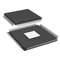
... SEATING 0.05 0.08 MAX PLANE COPLANARITY VIEW A ROTATED 90 ° CCW ORDERING GUIDE Model Temperature Range 1 AD8159ASVZ −40°C to +85°C AD8159-EVAL- RoHS Compliant Part. 16.00 BSC SQ 14.00 BSC SQ 76 100 PIN 1 TOP VIEW (PINS DOWN) 51 ...
Page 22
AD8159 NOTES Rev Page ...
Page 23
NOTES Rev Page AD8159 ...
Page 24
AD8159 NOTES ©2005–2009 Analog Devices, Inc. All rights reserved. Trademarks and registered trademarks are the property of their respective owners. D05611-0-5/09(B) Rev Page ...