AD8159ASVZ Analog Devices Inc, AD8159ASVZ Datasheet - Page 2
AD8159ASVZ
Manufacturer Part Number
AD8159ASVZ
Description
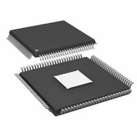
IC MUX/DEMUX QUAD BUFF 100TQFP
Manufacturer
Analog Devices Inc
Series
XStream™r
Datasheet
1.AD8159ASVZ.pdf
(24 pages)
Specifications of AD8159ASVZ
Applications
2:1 Multiplexer/1:2 De-Multiplexer
Interface
Serial
Voltage - Supply
3 V ~ 3.6 V
Package / Case
100-TQFP Exposed Pad, 100-eTQFP, 100-HTQFP, 100-VQFP
Mounting Type
Surface Mount
Crosspoint Switch Type
Digital
Input / Output Configuration
LVPECL, CML / CML
Control Interface
Parallel
Supply Voltage Range
3V To 3.6V
Operating Temperature Range
-40°C To +85°C
Lead Free Status / RoHS Status
Lead free / RoHS Compliant
Available stocks
Company
Part Number
Manufacturer
Quantity
Price
Company:

Part Number:
AD8159ASVZ
Manufacturer:
Analog Devices Inc
Quantity:
135
Company:
Part Number:
AD8159ASVZ
Manufacturer:
AnalogDevices
Quantity:
321
Company:
Part Number:
AD8159ASVZ
Manufacturer:
ADI
Quantity:
174
Company:
Part Number:
AD8159ASVZ
Manufacturer:
Analog Devices Inc
Quantity:
10 000
Part Number:
AD8159ASVZ
Manufacturer:
ADI/亚德诺
Quantity:
20 000


AD8159
TABLE OF CONTENTS
Features .............................................................................................. 1
Applications ....................................................................................... 1
General Description ......................................................................... 1
Functional Block Diagram .............................................................. 1
Revision History ............................................................................... 2
Specifications ..................................................................................... 3
Absolute Maximum Ratings ............................................................ 4
Pin Configuration and Function Descriptions ............................. 5
Typical Performance Characteristics ............................................. 8
Evaluation Board Simplified Block Diagrams ............................ 13
Test Circuits ..................................................................................... 14
REVISION HISTORY
5/09—Rev. A to Rev. B
Changes to Input Voltage Swing Parameter, Table 1 .................... 3
Added V
Changes to Table 3 ............................................................................ 5
Changes to Figure 24 ...................................................................... 11
Deleted Figure 30; Renumbered Sequentially ............................ 12
Deleted Figure 33 ............................................................................ 13
Changes to Figure 32 ...................................................................... 14
Changes to Table 5 and Table 6 ..................................................... 15
Deleted Table 7, Table 8, Table 10, and Table 11 ........................ 16
Changes to Applications Information Section ............................ 18
Changes to Termination Structures Section, Figure 39,
Figure 40, and Figure 42 ................................................................ 19
Added Figure 41; Renumbered Sequentially .............................. 19
Deleted DC Coupling Section and Figure 44 ............................. 20
Changes to Output Compliance Section ..................................... 20
Added Figure 43, Table 9, Table 10, and Table 11 ...................... 20
Deleted AC Coupling Section, Output Compliance Table
Section, and Table 13 ...................................................................... 21
Added Exposed Pad Notation to Outline Dimensions ............. 21
Changes to Ordering Guide .......................................................... 21
ESD Caution .................................................................................. 4
TTI
, V
TTO
, V
TTIO
, V
TTOI
Parameter, Table 1 ....................... 3
Rev. B | Page 2 of 24
Theory of Operation ...................................................................... 15
Applications Information .............................................................. 18
Interfacing to the AD8159 ............................................................. 19
Outline Dimensions ....................................................................... 21
4/06—Rev. 0 to Rev. A
Changes to Applications Section ..................................................... 1
Changes to Table 5 .......................................................................... 15
Updates to Outline Dimensions ................................................... 22
Changes to Ordering Guide .......................................................... 22
9/05—Revision 0: Initial Version
Input Equalization (EQ) and Output Pre-Emphasis (PE) .... 15
Loopback ..................................................................................... 16
Port C Reverse (Crossover) Capability .................................... 17
Termination Structures .............................................................. 19
Input Compliance ....................................................................... 19
Output Compliance ................................................................... 20
Ordering Guide .......................................................................... 21
Related parts for AD8159ASVZ
Image
Part Number
Description
Manufacturer
Datasheet
Request
R

Part Number:
Description:
SENSOR GAS FOR CO/NO2 EXHAUST
Manufacturer:
GE Sensing
Datasheet:

Part Number:
Description:
±1.7g Dual-Axis IMEMS Accelerometer Evaluation Board
Manufacturer:
Analog Devices Inc
Datasheet:

Part Number:
Description:
Inertial Sensor Evaluation System
Manufacturer:
Analog Devices Inc
Datasheet:
Part Number:
Description:
Manufacturer:
Analog Devices Inc
Datasheet:
Part Number:
Description:
Manufacturer:
Analog Devices Inc
Datasheet:
Part Number:
Description:
Manufacturer:
Analog Devices Inc
Datasheet:
Part Number:
Description:
Manufacturer:
Analog Devices Inc
Datasheet:
Part Number:
Description:
Manufacturer:
Analog Devices Inc
Datasheet:
Part Number:
Description:
Manufacturer:
Analog Devices Inc
Datasheet:
Part Number:
Description:
Manufacturer:
Analog Devices Inc
Datasheet:
Part Number:
Description:
Manufacturer:
Analog Devices Inc
Datasheet:
Part Number:
Description:
Manufacturer:
Analog Devices Inc
Datasheet:
Part Number:
Description:
Manufacturer:
Analog Devices Inc
Datasheet: