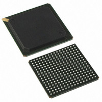
PI7C9X20508GPBNDE Pericom Semiconductor, PI7C9X20508GPBNDE Datasheet - Page 12

PI7C9X20508GPBNDE
Manufacturer Part Number
PI7C9X20508GPBNDE
Description
IC PCIE PACKET SWITCH 256BGA
Manufacturer
Pericom Semiconductor
Series
GreenPacket™r
Specifications of PI7C9X20508GPBNDE
Applications
Data Transport
Interface
Advanced Configuration Power Interface (ACPI)
Package / Case
256-PBGA
Mounting Type
Surface Mount
Lead Free Status / RoHS Status
Lead free / RoHS Compliant
Voltage - Supply
-
Available stocks
Company
Part Number
Manufacturer
Quantity
Price
Company:
Part Number:
PI7C9X20508GPBNDE
Manufacturer:
Pericom
Quantity:
200
3
3.1 PCI EXPRESS INTERFACE SIGNALS
3.2 PORT CONFIGURATION SIGNALS
June 2009 – Revision 1.5
Pericom Semiconductor
PIN DESCRIPTION
NAME
REFCLKP
REFCLKN
PERP [7:0]
PERN [7:0]
PETP [7:0]
PETN [7:0]
WAKEUP_L
RESET_L
DWNRST_L [4:1]
NAME
VC1_EN
SLOT_IMP [4:1]
F4
A16
A15
D16, K16,
M15, T13,
E1, B5, A7,
A13
D15, K15,
M16, T12,
E2, A5, B7,
B13
F15, H15,
P16, T15, C1,
A3, A9, A11
F16, H16,
P15, T16, B1,
B3, B9, B11
F2
E4
E5, D5, E6,
D6
*T6, G4, G2,
G1
PIN
PIN
TYPE
TYPE
O
O
O
I
I
I
I
I
I
I
Page 12 of 81
DESCRIPTION
Reference Clock Input Pairs: Connect to external 100MHz
differential clock.
The input clock signals must be delivered to the clock buffer cell
through an AC-coupled interface so that only the AC information of
the clock is received, converted, and buffered. It is recommended that a
0.1uF be used in the AC-coupling.
PCI Express Data Serial Input Pairs: Differential data receive
signals in five ports.
Port 0 (Upstream Port) is PERP[3:0] and PERN[3:0]
Port 1 (Downstream Port) is PERP[4] and PERN[4]
Port 2 (Downstream Port) is PERP[5] and PERN[5]
Port 3 (Downstream Port) is PERP[6] and PERN[6]
Port 4 (Downstream Port) is PERP[7] and PERN[7]
PCI Express Data Serial Output Pairs: Differential data transmit
signals in five ports.
Port 0 (Upstream Port) is PETP[3:0] and PETN[3:0]
Port 1 (Downstream Port) is PETP[4] and PETN[4]
Port 2 (Downstream Port) is PETP[5] and PETN[5]
Port 3 (Downstream Port) is PETP[6] and PETN[6]
Port 4 (Downstream Port) is PETP[7] and PETN[7]
Wakeup Signal (Active LOW): When WAKEUP_L is asserted, the
upstream port has to generate a Beacon that is propagated to the Root
Complex/Power Management Controller. Pin has an internal pull-up.
System Reset (Active LOW): When RESET_L is asserted, the
internal states of whole chip except sticky logics are initialized.
Downstream Device Reset (Active LOW): It provides a reset signal
to the devices connected to the downstream ports of switch. The signal
is active when either RESET_L is asserted or the device is just plugged
into the switch. DWNRST_L [x] corresponds to Portx, where x=
1,2,3,4.
DESCRIPTION
Virtual Channel 1Resource SharingEnable: The chip provides the
capability to support virtual channel 1 (VC1), in addition to the
standard virtual channel 0. When this pin is asserted high, Virtual
Channel 1 is enabled, and virtual channel resource sharing is not
available. When it is asserted low, the chip would allocate the
additional VC1 resource to VC0, and VC1 capability is disabled. The
pin has internal pull-down.
Slot Implemented: It decides if the downstream port is connected to
slot. SLOT_IMP [x] is correspondent to Portx, where x= 1,2,3,4. When
SLOT_IMP [x] is high, the Portx is connected to slot. The strapping
pin SLOT_IMP[4] is shared with PWR_IND[1]. By default,
downstream Port1, Port2, Port3, and Port4 are implemented with slots.
Pins are set to “1110” by default. SLOT_IMP[4] has internal pull-
down, and SLOT_IMP[3:1] have internal pull-up.
5Port-8Lane PCI Express Switch
GreenPacket
PI7C9X20508GP
Datasheet
TM
Family


