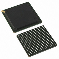
PI7C9X20508GPBNDE Pericom Semiconductor, PI7C9X20508GPBNDE Datasheet - Page 73

PI7C9X20508GPBNDE
Manufacturer Part Number
PI7C9X20508GPBNDE
Description
IC PCIE PACKET SWITCH 256BGA
Manufacturer
Pericom Semiconductor
Series
GreenPacket™r
Specifications of PI7C9X20508GPBNDE
Applications
Data Transport
Interface
Advanced Configuration Power Interface (ACPI)
Package / Case
256-PBGA
Mounting Type
Surface Mount
Lead Free Status / RoHS Status
Lead free / RoHS Compliant
Voltage - Supply
-
Available stocks
Company
Part Number
Manufacturer
Quantity
Price
Company:
Part Number:
PI7C9X20508GPBNDE
Manufacturer:
Pericom
Quantity:
200
10.4 BOUNDARY SCAN REGISTER
10.5 JTAG BOUNDARY SCAN REGISTER ORDER
June 2009 – Revision 1.5
Pericom Semiconductor
The boundary scan register has a set of serial shift-register cells. A chain of boundary scan cells is formed by
connected the internal signal of the PI7C9X20508GP package pins. The VDD, VSS, and JTAG pins are not
in the boundary scan chain. The input to the shift register is TDI and the output from the shift register is
TDO. There are 4 different types of boundary scan cells, based on the function of each signal pin.
The boundary scan register cells are dedicated logic and do not have any system function. Data may be
loaded into the boundary scan register master cells from the device input pins and output pin-drivers in
parallel by the mandatory SAMPLE and EXTEST instructions. Parallel loading takes place on the rising
edge of TCK.
Table 10-3 JTAG boundary scar register definition
Register Number
Boundary Scan
10
11
12
13
14
15
16
17
18
19
20
21
22
23
24
25
26
27
28
29
30
31
32
33
34
35
36
37
0
1
2
3
4
5
6
7
8
9
DWNRST_L[2]
DEBUG_OUT[10]
DEBUG_OUT[11]
DEBUG_OUT[0]
DEBUG_OUT[1]
DEBUG_OUT[2]
DEBUG_OUT[3]
DEBUG_OUT[4]
DEBUG_OUT[5]
DEBUG_OUT[6]
DEBUG_OUT[7]
DEBUG_OUT[8]
DEBUG_OUT[9]
DWNRST_L[1]
DWNRST_L[3]
CLKREQ1_L
CLKREQ2_L
CLKREQ3_L
PWR_IND[1]
Pin Name
PERST_L
WAKE_L
GPIO[0]
GPIO[1]
GPIO[2]
GPIO[3]
GPIO[4]
GPIO[5]
GPIO[6]
GPIO[7]
Page 73 of 81
Ball Location
H14
D15
A15
A14
A13
A12
A11
A10
H15
N14
L14
K14
G14
D16
C16
C15
C14
B16
B15
B14
A16
B13
B12
B11
B10
P11
P12
P13
D2
5Port-8Lane PCI Express Switch
Output2
Output2
Output2
Output2
Control
Control
Control
Control
Control
Control
Control
Control
Control
Type
Input
Input
Input
Input
Input
Bidir
Bidir
Bidir
Bidir
Bidir
Bidir
Bidir
Bidir
Bidir
Bidir
Bidir
Bidir
Bidir
Bidir
Bidir
Bidir
Bidir
Bidir
Bidir
Bidir
GreenPacket
PI7C9X20508GP
Tri-state Control Cell
Datasheet
TM
14
14
14
14
14
14
14
14
14
14
14
14
22
24
26
28
30
32
34
36
Family


