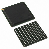
PI7C9X20508GPBNDE Pericom Semiconductor, PI7C9X20508GPBNDE Datasheet - Page 26

PI7C9X20508GPBNDE
Manufacturer Part Number
PI7C9X20508GPBNDE
Description
IC PCIE PACKET SWITCH 256BGA
Manufacturer
Pericom Semiconductor
Series
GreenPacket™r
Specifications of PI7C9X20508GPBNDE
Applications
Data Transport
Interface
Advanced Configuration Power Interface (ACPI)
Package / Case
256-PBGA
Mounting Type
Surface Mount
Lead Free Status / RoHS Status
Lead free / RoHS Compliant
Voltage - Supply
-
Available stocks
Company
Part Number
Manufacturer
Quantity
Price
Company:
Part Number:
PI7C9X20508GPBNDE
Manufacturer:
Pericom
Quantity:
200
6.1.4 MAPPING EEPROM CONTENTS TO CONFIGURATION REGISTERS
June 2009 – Revision 1.5
Pericom Semiconductor
ADDRESS
0Ah
0Ch
00h
02h
04h
06h
08h
Reserved
Reserved
Reserved
Reserved
Reserved
15 – 8
00h ~ 01h
02h ~ 03h
144h (Port 0~4)
144h: Bit [0]
ECh (Port 0~4)
ECh: Bit [14:12]
ECh: Bit [17:15]
B4h (Port 0~4)
B4h:Bit [5]
3Ch (Port 1~4)
3Ch: Bit [8]
BCh: Bit [15:0]
BCh: Bit [31:16]
E4h(Port 0~4)
E4h: Bit 0
ECh(Port 0~4)
ECh: Bit[11:10]
E4h(Port 0~4)
E4h: Bit[15]
B0h(port 0~4)
B0h : Bit [14]
B0h(port 0~4)
B0h : Bit [15]
B4h(port 0~4)
B4h : Bit [15]
B0h(port 0~4)
Bit [6]
Bit [0]
Bit [2:1]
Bit [3]
Bit [4]
PCI CFG
OFFSET
PHY Parameter for Port 1
PHY Parameter for Port 2
PHY Parameter for Port 3
PHY Parameter for Port 4
Reserved
Reserved
Reserved
DESCRIPTION
EEPROM signature – 1516h
Vendor ID
Device ID
Extended VC Count for Port 0 ~ 4
Link Capability for Port 0 ~ 4
Switch Mode Operation for Port 0
Interrupt pin for Port 1 ~ 4
Subsystem Vender ID
Subsystem ID
Max_Payload_Size Support for Port 0 ~ 4
ASPM Support for Port 0 ~ 4
Role_Base Error Reporting for Port 0 ~ 4
MSI Capability Disable for Port 0~4
AER Capability Disable for Port 0~4
Compliance Pattern Parity Control Disable for Port 0~4
Power Management Capability Disable for Port 0~4
PM Control Para/Rx Polarity for Port 0
PM Control Para/Rx Polarity for Port 1
PM Control Para/Rx Polarity for Port 2
PM Control Para/Rx Polarity for Port 3
PM Control Para/Rx Polarity for Port 4
Page 26 of 81
Bit [0]: It represents the supported VC count other than the
default VC
Bit [3:1]: It represents L0s Exit Latency for all ports
Bit [6:4]: It represents L1 Exit Latency for all ports
Bit [8]: no ordering on packets for different egress port mode
Bit [9]: no ordering on different tag of completion mode
Bit [10]: Store and Forward
Bit [12:11]: Cut-through Threshold
Bit [13] : Port arbitrator Mode
Bit [14]: Credit Update Mode
Bit [15]: Set when INTA is requested for interrupt resource
Bit [0]: Indicated the maximum payload size that the device can
support for the TLP
Bit [2:1] : Indicate the level of ASPM supported on the PCIe link
Bit [3] : Indicate implement the role-base error reporting
Bit [4] : Disable MSI capability
Bit [5] : Disable AER capability
Bit [6] : Disable compliance pattern parity
7 – 0
5Port-8Lane PCI Express Switch
GreenPacket
BYTE OFFSET
PI7C9X20508GP
9Ah
A0h
A2h
A4h
A6h
A8h
9Ch
9Eh
92h
94h
96h
98h
Datasheet
TM
Family


