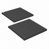
DS33X81+ Maxim Integrated Products, DS33X81+ Datasheet - Page 244

DS33X81+
Manufacturer Part Number
DS33X81+
Description
IC MAPPING ETHERNET 256CSBGA
Manufacturer
Maxim Integrated Products
Datasheet
1.DS33X11.pdf
(375 pages)
Specifications of DS33X81+
Applications
Data Transport
Interface
Parallel/Serial
Voltage - Supply
1.8V, 2.5V, 3.3V
Package / Case
256-CSBGA
Mounting Type
Surface Mount
Lead Free Status / RoHS Status
Lead free / RoHS Compliant
- Current page: 244 of 375
- Download datasheet (3Mb)
323h:
Default
Register Name:
Register Description:
Register Address:
322h:
Default
Note – bit definitions below not symmetric Decap/Encap:
Bit 3: Decapsulator Error Mode (DEM) When set to 1, errored frames are forwarded. Normally they are
discarded. This bit function was located in DMCR bit 0 in device revision A1 (GL.IDR.REVn=000).
Bit 2: Decapsulator State Machine Reset (DSMRE) If this bit is set and DFSRWPC transitions, The
Decapsulator State Machine will be reset.
Bit 1: Decapsulator FIFO Pointer reset Enable (DFPRE) - Setting this bit to a 1 will enable the FIFO to be reset.
The FIFO Read and Write pointer will be reset if DFSRWPC transitions and this bit is set.
Bit 0: Decapsulator FIFO and State Read, Write, and PMU Control (DFSRWPC)- A 0 to 1 transition enables the
FIFO Read and Write Addresses, Status Registers to be read by the processor. The user must wait 4 system
clocks before the reads can be done. This bit is used to control resetting of the FIFO Read and Write Pointers and
the Decapsulator State Machine. This bit is also used as a PMU update for all decapsulator latched counters.
Rev: 063008
________________________________________________ DS33X162/X161/X82/X81/X42/X41/X11/W41/W11
Bit 15
Bit 7
0
0
-
-
Bit 14
Bit 6
0
0
-
-
PP.DFSCR
Decapsulator FIFO Control Register
322h (+ 040h x (n-1), WAN Group Decapsulator n=1 to 4)
Bit 13
Bit 5
0
0
-
-
Bit 12
Bit 4
0
0
-
-
Bit 11
Bit 3
DEM
0
0
-
DSMRE
Bit 10
Bit 2
0
0
-
DFPRE
Bit 9
Bit 1
0
0
-
DFSRWPC
244 of 375
Bit 8
Bit 0
0
0
-
Related parts for DS33X81+
Image
Part Number
Description
Manufacturer
Datasheet
Request
R

Part Number:
Description:
MAX7528KCWPMaxim Integrated Products [CMOS Dual 8-Bit Buffered Multiplying DACs]
Manufacturer:
Maxim Integrated Products
Datasheet:

Part Number:
Description:
Single +5V, fully integrated, 1.25Gbps laser diode driver.
Manufacturer:
Maxim Integrated Products
Datasheet:

Part Number:
Description:
Single +5V, fully integrated, 155Mbps laser diode driver.
Manufacturer:
Maxim Integrated Products
Datasheet:

Part Number:
Description:
VRD11/VRD10, K8 Rev F 2/3/4-Phase PWM Controllers with Integrated Dual MOSFET Drivers
Manufacturer:
Maxim Integrated Products
Datasheet:

Part Number:
Description:
Highly Integrated Level 2 SMBus Battery Chargers
Manufacturer:
Maxim Integrated Products
Datasheet:

Part Number:
Description:
Current Monitor and Accumulator with Integrated Sense Resistor; ; Temperature Range: -40°C to +85°C
Manufacturer:
Maxim Integrated Products

Part Number:
Description:
TSSOP 14/A�/RS-485 Transceivers with Integrated 100O/120O Termination Resis
Manufacturer:
Maxim Integrated Products

Part Number:
Description:
TSSOP 14/A�/RS-485 Transceivers with Integrated 100O/120O Termination Resis
Manufacturer:
Maxim Integrated Products

Part Number:
Description:
QFN 16/A�/AC-DC and DC-DC Peak-Current-Mode Converters with Integrated Step
Manufacturer:
Maxim Integrated Products

Part Number:
Description:
TDFN/A/65V, 1A, 600KHZ, SYNCHRONOUS STEP-DOWN REGULATOR WITH INTEGRATED SWI
Manufacturer:
Maxim Integrated Products

Part Number:
Description:
Integrated Temperature Controller f
Manufacturer:
Maxim Integrated Products

Part Number:
Description:
SOT23-6/I�/45MHz to 650MHz, Integrated IF VCOs with Differential Output
Manufacturer:
Maxim Integrated Products

Part Number:
Description:
SOT23-6/I�/45MHz to 650MHz, Integrated IF VCOs with Differential Output
Manufacturer:
Maxim Integrated Products

Part Number:
Description:
EVALUATION KIT/2.4GHZ TO 2.5GHZ 802.11G/B RF TRANSCEIVER WITH INTEGRATED PA
Manufacturer:
Maxim Integrated Products

Part Number:
Description:
QFN/E/DUAL PCIE/SATA HIGH SPEED SWITCH WITH INTEGRATED BIAS RESISTOR
Manufacturer:
Maxim Integrated Products
Datasheet:


