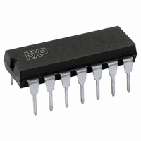
74HCT4016N,112 NXP Semiconductors, 74HCT4016N,112 Datasheet - Page 9

74HCT4016N,112
Manufacturer Part Number
74HCT4016N,112
Description
IC SWITCH QUAD SPST 14DIP
Manufacturer
NXP Semiconductors
Series
74HCTr
Datasheets
1.74HCT4046ADB112.pdf
(19 pages)
2.74HCT4046ADB112.pdf
(23 pages)
3.74HCT4016N112.pdf
(14 pages)
Specifications of 74HCT4016N,112
Package / Case
14-DIP (0.300", 7.62mm)
Function
Switch
Circuit
4 x SPST - NO
On-state Resistance
80 Ohm
Voltage Supply Source
Single Supply
Voltage - Supply, Single/dual (±)
4.5 V ~ 5.5 V
Current - Supply
2µA
Mounting Type
Through Hole
Switch Configuration
SPST
On Resistance (max)
320 Ohm @ 4.5 V
On Time (max)
35 ns @ 4.5 V
Off Time (max)
35 ns @ 4.5 V
Supply Voltage (max)
5.5 V
Supply Voltage (min)
4.5 V
Maximum Power Dissipation
750 mW
Maximum Operating Temperature
+ 125 C
Mounting Style
Through Hole
Minimum Operating Temperature
- 40 C
Lead Free Status / RoHS Status
Lead free / RoHS Compliant
Lead Free Status / RoHS Status
Lead free / RoHS Compliant, Lead free / RoHS Compliant
Other names
568-2845-5
933668980112
933668980112
Philips Semiconductors
DC CHARACTERISTICS FOR 74HCT
Voltages are referenced to GND (ground = 0 V)
Note
1. The value of additional quiescent supply current ( I
December 1990
SYMBOL
V
V
I
INPUT
E
CC
I
I
I
I
IH
IL
N
Quad bilateral switches
I
S
S
CC
To determine I
UNIT LOAD COEFFICIENT
1.00
PARAMETER
HIGH level input
voltage
LOW level input
voltage
input leakage
current
analog switch
OFF-state current
per channel
analog switch
ON-state current
quiescent supply
current
additional quiescent
supply current per
input pin for unit
load coefficient is 1
(note 1)
CC
per input, multiply this value by the unit load coefficient shown in the table below.
2.0
min. typ. max. min. max. min.
1.6
1.2
100
25
0.8
0.1
0.1
0.1
2.0
360
T
74HCT
amb
2.0
CC
40 to 85
) for a unit load of 1 is given here.
9
( C)
0.8
1.0
1.0
1.0
20.0
450
2.0
40 to 125
0.8
1.0
1.0
1.0
40.0
490
max.
UNIT
V
V
A
A
A
A
A
TEST CONDITIONS
V
4.5
to
5.5
4.5
to
5.5
5.5
5.5
5.5
4.5
to
5.5
4.5
to
5.5
(V)
74HC/HCT4016
CC
V
V
or
GND
V
or
V
V
or
V
V
or
GND
V
Product specification
2.1V
I
CC
IH
IL
IH
IL
CC
CC
OTHER
V
(see Fig.7)
V
(see Fig.8)
V
V
V
other inputs
at V
GND
V
V
CC
CC
is
CC
CC
S
S
= GND or
; V
CC
or GND
=
=
GND
GND
os
or
=


