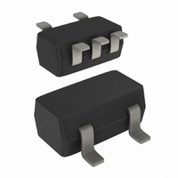
74LVC1G384GW,125 NXP Semiconductors, 74LVC1G384GW,125 Datasheet - Page 7

74LVC1G384GW,125
Manufacturer Part Number
74LVC1G384GW,125
Description
IC SWITCH SPST UMT5
Manufacturer
NXP Semiconductors
Series
74LVCr
Type
Analog Switchr
Datasheet
1.74LVC1G384GV125.pdf
(25 pages)
Specifications of 74LVC1G384GW,125
Package / Case
6-TSSOP (5 lead), SC-88A, SOT-353
Function
Switch
Circuit
1 x SPST- NO
On-state Resistance
6 Ohm
Voltage Supply Source
Single Supply
Voltage - Supply, Single/dual (±)
1.65 V ~ 5.5 V
Current - Supply
0.1µA
Operating Temperature
-40°C ~ 125°C
Mounting Type
Surface Mount
Switch Configuration
SPST
On Resistance (max)
34 Ohm (Typ) @ 1.95 V
On Time (max)
10 ns (Typ) @ 1.95 V
Off Time (max)
7.4 ns (Typ) @ 1.95 V
Supply Voltage (max)
5.5 V
Supply Voltage (min)
1.65 V
Maximum Power Dissipation
250 mW
Maximum Operating Temperature
+ 125 C
Mounting Style
SMD/SMT
Minimum Operating Temperature
- 40 C
Switch Current (typ)
0.0001 mA @ 3.3 V
Multiplexer Configuration
Single SPST
Number Of Inputs
1
Number Of Outputs
1
Number Of Channels
1
Analog Switch On Resistance
34@1.95VOhm
Power Supply Requirement
Single
Single Supply Voltage (min)
1.65V
Single Supply Voltage (typ)
3/5V
Single Supply Voltage (max)
5.5V
Dual Supply Voltage (min)
Not RequiredV
Dual Supply Voltage (typ)
Not RequiredV
Dual Supply Voltage (max)
Not RequiredV
Power Dissipation
250mW
Mounting
Surface Mount
Pin Count
5
Operating Temp Range
-40C to 125C
Operating Temperature Classification
Automotive
Lead Free Status / RoHS Status
Lead free / RoHS Compliant
Lead Free Status / RoHS Status
Lead free / RoHS Compliant, Lead free / RoHS Compliant
Other names
74LVC1G384GW-G
74LVC1G384GW-G
935274581125
74LVC1G384GW-G
935274581125
NXP Semiconductors
Table 8.
At recommended operating conditions; voltages are referenced to GND (ground 0 V); for graphs see
[1]
[2]
74LVC1G384
Product data sheet
Symbol
R
Fig 9.
ON(flat)
Typical values are measured at T
Flatness is defined as the difference between the maximum and minimum value of ON resistance measured at identical V
temperature.
R
V
Test circuit for measuring ON resistance
Parameter
ON resistance
(flatness)
IL
ON
ON resistance
= V
V I
10.3 ON resistance test circuit and graphs
SW
/ I
E
Y
SW
.
…continued
V
V
SW
CC
GND
amb
Conditions
V
Z
I
I
V
I
I
I
I
= 25 °C and nominal V
= GND to V
SW
SW
SW
SW
SW
CC
= 4 mA;
= 8 mA; V
= 12 mA; V
= 24 mA; V
= 32 mA; V
= 1.65 V to 1.95 V
001aag481
All information provided in this document is subject to legal disclaimers.
I SW
Rev. 3 — 3 November 2010
CC
CC
CC
CC
CC
= 2.3 V to 2.7 V
= 2.7 V
= 3 V to 3.6 V
= 4.5 V to 5.5 V
CC
.
Fig 10. Typical ON resistance as a function of input
R
(Ω)
(1) V
(2) V
(3) V
(4) V
(5) V
ON
40
30
20
10
0
0
voltage; T
[2]
CC
CC
CC
CC
CC
= 1.8 V.
= 2.5 V.
= 2.7 V.
= 3.3 V.
= 5.0 V.
(1)
Min
−40 °C to +85 °C
-
-
-
-
-
(2)
(3)
1
amb
Typ
26.0
5.0
3.5
2.0
1.5
(4)
= 25 °C
[1]
2
Max
74LVC1G384
-
-
-
-
-
3
−40 °C to +125 °C Unit
Figure 10
Min
-
-
-
-
-
© NXP B.V. 2010. All rights reserved.
(5)
4
Bilateral switch
V
mna673
I
(V)
Max
to
CC
-
-
-
-
-
5
Figure
and
7 of 25
Ω
Ω
Ω
Ω
Ω
15.


