74LV4051D,118 NXP Semiconductors, 74LV4051D,118 Datasheet - Page 4
74LV4051D,118
Manufacturer Part Number
74LV4051D,118
Description
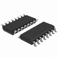
IC MUX/DEMUX 8X1 16SOIC
Manufacturer
NXP Semiconductors
Series
74LVr
Type
Analog Multiplexerr
Datasheet
1.74LV4051PW118.pdf
(26 pages)
Specifications of 74LV4051D,118
Package / Case
16-SOIC (0.154", 3.90mm Width)
Function
Multiplexer/Demultiplexer
Circuit
1 x 8:1
On-state Resistance
60 Ohm
Current - Supply
80µA
Operating Temperature
-40°C ~ 125°C
Mounting Type
Surface Mount
Propagation Delay Time
23 ns
Supply Voltage (max)
6 V
Supply Voltage (min)
1 V
Maximum Operating Temperature
+ 125 C
Minimum Operating Temperature
- 40 C
Mounting Style
SMD/SMT
Package
16SO
Maximum On Resistance
375@2V Ohm
Maximum Propagation Delay Bus To Bus
25(Typ)@1.2V|9(Typ)@2V|6(Typ)@2.7V|5(Typ)@3.3V|4(Typ)@4.5V|3(Typ)@6V ns
Maximum High Level Output Current
25 mA
Multiplexer Architecture
8:1
Maximum Turn-on Time
145(Typ)@1.2V ns
Power Supply Type
Single
Lead Free Status / RoHS Status
Lead free / RoHS Compliant
Lead Free Status / RoHS Status
Lead free / RoHS Compliant, Lead free / RoHS Compliant
Other names
74LV4051D-T
74LV4051D-T
935190970118
74LV4051D-T
935190970118
Available stocks
Company
Part Number
Manufacturer
Quantity
Price

Part Number:
74LV4051D,118
Manufacturer:
NXP/恩智浦
Quantity:
20 000


NXP Semiconductors
5. Pinning information
Table 2.
74LV4051_4
Product data sheet
Symbol
E
V
GND
S0, S1, S2
Y0, Y1, Y2, Y3, Y4, Y5, Y6, Y7 13, 14, 15, 12, 1, 5, 2, 4 independent input or output
Z
V
Fig 5.
EE
CC
GND
V
Y4
Y6
Y7
Y5
EE
E
Z
Pin configuration SOT38-4
and SOT109-1
Pin description
1
2
3
4
5
6
7
8
74LV4051
5.1 Pinning
5.2 Pin description
001aak433
16
15
14
13
12
11
10
9
V
Y2
Y1
Y0
Y3
S0
S1
S2
CC
Pin
6
7
8
11, 10, 9
3
16
Fig 6.
GND
V
Y4
Y6
Y7
Y5
EE
E
Z
1
2
3
4
5
6
7
8
Rev. 04 — 10 August 2009
Pin configuration
SOT338-1 and SOT403-1
Description
enable input (active LOW)
supply voltage
ground supply voltage
select input
common output or input
supply voltage
74LV4051
001aak407
8-channel analog multiplexer/demultiplexer
16
15
14
13
12
11
10
9
V
Y2
Y1
Y0
Y3
S0
S1
S2
CC
Fig 7.
index area
terminal 1
V
Y6
Y7
Y5
EE
Pin configuration for
SOT763-1
E
Z
Transparent top view
2
3
4
5
6
7
74LV4051
74LV4051
V
CC
© NXP B.V. 2009. All rights reserved.
(1)
15
14
13
12
11
10
001aak408
Y2
Y1
Y0
Y3
S0
S1
4 of 26
Related parts for 74LV4051D,118
Image
Part Number
Description
Manufacturer
Datasheet
Request
R

Part Number:
Description:
NXP Semiconductors designed the LPC2420/2460 microcontroller around a 16-bit/32-bitARM7TDMI-S CPU core with real-time debug interfaces that include both JTAG andembedded trace
Manufacturer:
NXP Semiconductors
Datasheet:

Part Number:
Description:
NXP Semiconductors designed the LPC2458 microcontroller around a 16-bit/32-bitARM7TDMI-S CPU core with real-time debug interfaces that include both JTAG andembedded trace
Manufacturer:
NXP Semiconductors
Datasheet:
Part Number:
Description:
NXP Semiconductors designed the LPC2468 microcontroller around a 16-bit/32-bitARM7TDMI-S CPU core with real-time debug interfaces that include both JTAG andembedded trace
Manufacturer:
NXP Semiconductors
Datasheet:
Part Number:
Description:
NXP Semiconductors designed the LPC2470 microcontroller, powered by theARM7TDMI-S core, to be a highly integrated microcontroller for a wide range ofapplications that require advanced communications and high quality graphic displays
Manufacturer:
NXP Semiconductors
Datasheet:
Part Number:
Description:
NXP Semiconductors designed the LPC2478 microcontroller, powered by theARM7TDMI-S core, to be a highly integrated microcontroller for a wide range ofapplications that require advanced communications and high quality graphic displays
Manufacturer:
NXP Semiconductors
Datasheet:
Part Number:
Description:
The Philips Semiconductors XA (eXtended Architecture) family of 16-bit single-chip microcontrollers is powerful enough to easily handle the requirements of high performance embedded applications, yet inexpensive enough to compete in the market for hi
Manufacturer:
NXP Semiconductors
Datasheet:
Part Number:
Description:
The XA-S3 device is a member of Philips Semiconductors? XA(eXtended Architecture) family of high performance 16-bitsingle-chip microcontrollers
Manufacturer:
NXP Semiconductors
Datasheet:

Part Number:
Description:
The NXP BlueStreak LH75401/LH75411 family consists of two low-cost 16/32-bit System-on-Chip (SoC) devices
Manufacturer:
NXP Semiconductors
Datasheet:
Part Number:
Description:
The NXP LPC3130/3131 combine an 180 MHz ARM926EJ-S CPU core, high-speed USB2
Manufacturer:
NXP Semiconductors
Datasheet:
Part Number:
Description:
The NXP LPC3141 combine a 270 MHz ARM926EJ-S CPU core, High-speed USB 2
Manufacturer:
NXP Semiconductors
Part Number:
Description:
The NXP LPC3143 combine a 270 MHz ARM926EJ-S CPU core, High-speed USB 2
Manufacturer:
NXP Semiconductors

Part Number:
Description:
The NXP LPC3152 combines an 180 MHz ARM926EJ-S CPU core, High-speed USB 2
Manufacturer:
NXP Semiconductors
Part Number:
Description:
The NXP LPC3154 combines an 180 MHz ARM926EJ-S CPU core, High-speed USB 2
Manufacturer:
NXP Semiconductors

Part Number:
Description:
Standard level N-channel enhancement mode Field-Effect Transistor (FET) in a plastic package using NXP High-Performance Automotive (HPA) TrenchMOS technology
Manufacturer:
NXP Semiconductors
Datasheet: