LFE3-35EA-8FN672I Lattice, LFE3-35EA-8FN672I Datasheet - Page 118
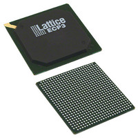
LFE3-35EA-8FN672I
Manufacturer Part Number
LFE3-35EA-8FN672I
Description
IC FPGA 33.3K LUTS 310I/O FN672
Manufacturer
Lattice
Series
ECP3r
Datasheets
1.LFE3-150EA-7FN672C.pdf
(136 pages)
2.LFE3-35EA-8FN672I.pdf
(4 pages)
3.LFE3-35EA-8FN672I.pdf
(21 pages)
Specifications of LFE3-35EA-8FN672I
Number Of Logic Elements/cells
33000
Number Of Labs/clbs
4125
Total Ram Bits
1358848
Number Of I /o
310
Number Of Gates
-
Voltage - Supply
1.14 V ~ 1.26 V
Mounting Type
Surface Mount
Operating Temperature
-40°C ~ 100°C
Package / Case
672-BBGA
Lead Free Status / Rohs Status
Lead free / RoHS Compliant
Other names
220-1163


Signal Descriptions (Cont.)
Lattice Semiconductor
D7/SPID0
DI/CSSPI0N/CEN
Dedicated SERDES Signals
PCS[Index]_HDINNm
PCS[Index]_HDOUTNm
PCS[Index]_REFCLKN
PCS[Index]_HDINPm
PCS[Index]_HDOUTPm
PCS[Index]_REFCLKP
PCS[Index]_VCCOBm
PCS[Index]_VCCIBm
1. When placing switching I/Os around these critical pins that are designed to supply the device with the proper reference or supply voltage,
2. m defines the associated channel in the quad.
care must be given.
Signal Name
2
I/O
I/O
I/O
—
—
O
O
I
I
I
I
Parallel configuration I/O. SPI/SPIm data input. Open drain during configura-
tion.
Serial data input for slave serial mode. SPI/SPIm mode chip select.
High-speed input, negative channel m
High-speed output, negative channel m
Negative Reference Clock Input
High-speed input, positive channel m
High-speed output, positive channel m
Positive Reference Clock Input
Output buffer power supply, channel m (1.2V/1.5)
Input buffer power supply, channel m (1.2V/1.5V)
4-3
Description
LatticeECP3 Family Data Sheet
Pinout Information
Related parts for LFE3-35EA-8FN672I
Image
Part Number
Description
Manufacturer
Datasheet
Request
R

Part Number:
Description:
33.3K LUTS, 295 I/O, 1.2V, -6 SPEED, PB-FREE
Manufacturer:
LATTICE SEMICONDUCTOR
Datasheet:
Part Number:
Description:
FPGA LatticeECP3™ Family 33000 Cells 65nm Technology 1.2V 484-Pin FBGA
Manufacturer:
LATTICE SEMICONDUCTOR
Datasheet:

Part Number:
Description:
IC FPGA 33.3KLUTS 133I/O 256BGA
Manufacturer:
Lattice
Datasheet:
Part Number:
Description:
IC FPGA 33.3KLUTS 133I/O 256BGA
Manufacturer:
Lattice
Datasheet:
Part Number:
Description:
IC FPGA 33.3KLUTS 295I/O 484BGA
Manufacturer:
Lattice
Datasheet:
Part Number:
Description:
IC FPGA 33.3KLUTS 310I/O 672BGA
Manufacturer:
Lattice
Datasheet:
Part Number:
Description:
IC FPGA 33.3KLUTS 310I/O 672BGA
Manufacturer:
Lattice
Datasheet:
Part Number:
Description:
IC FPGA 35KLUTS 133I/O 256-BGA
Manufacturer:
Lattice
Datasheet:
Part Number:
Description:
IC FPGA 35KLUTS 133I/O 256-BGA
Manufacturer:
Lattice
Datasheet:
Part Number:
Description:
IC FPGA 33KLUTS 295I/O 484-BGA
Manufacturer:
Lattice
Datasheet:
Part Number:
Description:
IC FPGA 33KLUTS 295I/O 484-BGA
Manufacturer:
Lattice
Datasheet:
Part Number:
Description:
IC FPGA 35KLUTS 133I/O 256-BGA
Manufacturer:
Lattice
Datasheet:
Part Number:
Description:
IC FPGA 33KLUTS 295I/O 484-BGA
Manufacturer:
Lattice
Datasheet:
Part Number:
Description:
IC FPGA 33.3KLUTS 672FPBGA
Manufacturer:
Lattice
Datasheet:
Part Number:
Description:
IC FPGA 33.3KLUTS 256FTBGA
Manufacturer:
Lattice
Datasheet: