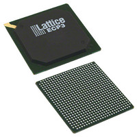
LFE3-35EA-8FN672I Lattice, LFE3-35EA-8FN672I Datasheet - Page 25

LFE3-35EA-8FN672I
Manufacturer Part Number
LFE3-35EA-8FN672I
Description
IC FPGA 33.3K LUTS 310I/O FN672
Manufacturer
Lattice
Series
ECP3r
Datasheets
1.LFE3-150EA-7FN672C.pdf
(136 pages)
2.LFE3-35EA-8FN672I.pdf
(4 pages)
3.LFE3-35EA-8FN672I.pdf
(21 pages)
Specifications of LFE3-35EA-8FN672I
Number Of Logic Elements/cells
33000
Number Of Labs/clbs
4125
Total Ram Bits
1358848
Number Of I /o
310
Number Of Gates
-
Voltage - Supply
1.14 V ~ 1.26 V
Mounting Type
Surface Mount
Operating Temperature
-40°C ~ 100°C
Package / Case
672-BBGA
Lead Free Status / Rohs Status
Lead free / RoHS Compliant
Other names
220-1163
- LFE3-150EA-7FN672C PDF datasheet
- LFE3-35EA-8FN672I PDF datasheet #2
- LFE3-35EA-8FN672I PDF datasheet #3
- Current page: 25 of 136
- Download datasheet (3Mb)
Lattice Semiconductor
For most cases, as shown in Figure 2-24, the LatticeECP3 DSP slice is backwards-compatible with the
LatticeECP2™ sysDSP block, such that, legacy applications can be targeted to the LatticeECP3 sysDSP slice. The
functionality of one LatticeECP2 sysDSP Block can be mapped into two adjacent LatticeECP3 sysDSP slices, as
shown in Figure 2-25.
Figure 2-24. Simplified sysDSP Slice Block Diagram
• RTL Synthesis friendly synchronous reset on all registers, while still supporting asynchronous reset for legacy
• Dynamic MUX selection to allow Time Division Multiplexing (TDM) of resources for applications that require
– Flexible cascading across slices to get larger functions
users
processor-like flexibility that enables different functions for each clock cycle
Intermediate Pipeline
as, overflow, underflow and convergent rounding, etc.
Output Registers
ALU Op-Codes
Input Registers
Left-side DSP
Cascade from
from SRO of
Registers
Left DSP
9x9
OR
Mult18-0
MULTA
Accumulator/ALU (54)
PR
IR
IR
9x9
OR
9x9
OR
Slice 0
Mult18-1
MULTB
PR
IR
IR
9x9
OR
From FPGA Core
To FPGA Core
Carry
Reg.
Out
2-22
Casc
A0
9x9
OR
Mult18-0
MULTA
Accumulator/ALU (54)
PR
IR
IR
9x9
OR
LatticeECP3 Family Data Sheet
Slice 1
9x9
OR
Mult18-1
MULTB
PR
IR
IR
9x9
OR
Carry
Reg.
Casc
Out
A1
One of
these
Architecture
Cascade to
Right DSP
Related parts for LFE3-35EA-8FN672I
Image
Part Number
Description
Manufacturer
Datasheet
Request
R
Part Number:
Description:
33.3K LUTS, 295 I/O, 1.2V, -6 SPEED, PB-FREE
Manufacturer:
LATTICE SEMICONDUCTOR
Datasheet:
Part Number:
Description:
FPGA LatticeECP3™ Family 33000 Cells 65nm Technology 1.2V 484-Pin FBGA
Manufacturer:
LATTICE SEMICONDUCTOR
Datasheet:

Part Number:
Description:
IC FPGA 33.3KLUTS 133I/O 256BGA
Manufacturer:
Lattice
Datasheet:

Part Number:
Description:
IC FPGA 33.3KLUTS 133I/O 256BGA
Manufacturer:
Lattice
Datasheet:

Part Number:
Description:
IC FPGA 33.3KLUTS 295I/O 484BGA
Manufacturer:
Lattice
Datasheet:

Part Number:
Description:
IC FPGA 33.3KLUTS 310I/O 672BGA
Manufacturer:
Lattice
Datasheet:

Part Number:
Description:
IC FPGA 33.3KLUTS 310I/O 672BGA
Manufacturer:
Lattice
Datasheet:

Part Number:
Description:
IC FPGA 35KLUTS 133I/O 256-BGA
Manufacturer:
Lattice
Datasheet:

Part Number:
Description:
IC FPGA 35KLUTS 133I/O 256-BGA
Manufacturer:
Lattice
Datasheet:

Part Number:
Description:
IC FPGA 33KLUTS 295I/O 484-BGA
Manufacturer:
Lattice
Datasheet:

Part Number:
Description:
IC FPGA 33KLUTS 295I/O 484-BGA
Manufacturer:
Lattice
Datasheet:

Part Number:
Description:
IC FPGA 35KLUTS 133I/O 256-BGA
Manufacturer:
Lattice
Datasheet:

Part Number:
Description:
IC FPGA 33KLUTS 295I/O 484-BGA
Manufacturer:
Lattice
Datasheet:

Part Number:
Description:
IC FPGA 33.3KLUTS 672FPBGA
Manufacturer:
Lattice
Datasheet:

Part Number:
Description:
IC FPGA 33.3KLUTS 256FTBGA
Manufacturer:
Lattice
Datasheet:


