03805-06-0100 IEE (INDUSTRIAL ELECTRONIC ENGINEERS), 03805-06-0100 Datasheet
03805-06-0100
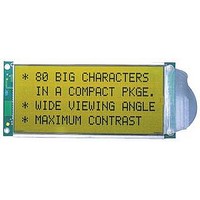
Specifications of 03805-06-0100


Related parts for 03805-06-0100


03805-06-0100 Summary of contents
Page 1
... REPRODUCED, OR COPIED OR USED AS THE BASIS FOR MANUFACTURE OR SALE OF APPARATUS WITHOUT APPROVED WRITTEN PERMISSION OF I.E.E. INC. LTR DESCRIPTION – PRODUCTION RELEASE/E.O. 29226 A E.O. 29434 B E.O. 29653 C E.O. 36743, Revised and Redrawn Specification Daystar Nova LCD Module With Parallel Data Input Option Model 03805–06–0100 REVISION STATUS 3– ...
Page 2
... Optical Characteristics ...............................................................................................................................16 6.2 Viewing Angle Adjustment...........................................................................................................................17 7.0 INSTALLATION NOTE ................................................................................................................................17 8.0 ACCESSORIES..........................................................................................................................................17 9.0 OUTLINE and INSTALLATION characteristics ...........................................................................................17 Industrial Electronic Engineers, Inc. Van Nuys, California Table of Contents Title = 5V ±10%)................................................................................................12 CC SIZE CODE IDENT A Scale: NONE S03805–06–0100 NO. 05464 Rev C Sheet 2 Page ...
Page 3
... Figure 14 Busy Flag Check Sequence for 4–bit Parallel Interface......................................................................14 Figure 15 Definition of Vertical Viewing Angle......................................................................................................17 Figure 16 Definition of Horizontal Viewing Angle..................................................................................................17 Figure 17 Definition of Contrast Ratio (CR).........................................................................................................17 Figure 18 Definition of Optical Response............................................................................................................17 Figure 19 03805–06–0100 Outline Drawing ........................................................................................................17 Industrial Electronic Engineers, Inc. Van Nuys, California List of Figures Title ...
Page 4
... Super Bi–refringent Effect (SBE) liquid crystal cell used in this display. For applications where the display is remotely located feet from the host processor, the serial data input option should be used. The serial option model is described in IEE specification S03805–06–0200. 1.3 Description The Daystar Nova module is a self– ...
Page 5
... LCD Column Drivers and Shift Registers LCD Controller Figure 1 Module Block Diagram Number Of Lines Input/Output SIZE CODE IDENT A Scale: NONE Temperature Compensation V (+5V) Gnd CC Connected I MPU I MPU I MPU I/O MPU I/O MPU – Power – – S03805–06–0100 NO. 05464 Rev C Sheet 5 ...
Page 6
... RAM) (CG ROM) 512 Bits 7200 Bits 5 5 Parallel/Serial Data Conversion Circuit (Parallel Data –Serial Data) Figure 2 LCD Controller Block Diagram SIZE CODE IDENT A Scale: NONE CL1 3 CL2 Com1–Com16 40 Seg1–Seg40 40–bit Shift Register D S03805–06–0100 NO. 05464 Rev C Sheet 6 ...
Page 7
... Character Generator RAM (CG RAM) The CG RAM allows the user to define 8 types character patterns. Figure 4 shows the relationship Industrial Electronic Engineers, Inc. Van Nuys, California SIZE CODE IDENT A NO. 05464 Scale: NONE Rev C S03805–06–0100 Sheet 7 ...
Page 8
... These blocks control the interface to the LCD drivers. Industrial Electronic Engineers, Inc. Van Nuys, California CG RAM Address Higher Order Bits Lower Order Bits SIZE CODE IDENT A Scale: NONE Character Patterns (CG RAM Data Higher Order Bits Lower Order Bits Character Pattern Example S03805–06–0100 NO. 05464 Rev C Sheet 8 Cursor ...
Page 9
... SIZE CODE IDENT A Scale: NONE Description Display Data RAM Character Generator RAM CG RAM Address CG DD RAM Address DD (Corresponds to cursor address) Address Counter (used for both CG and DD RAM) Don’t Care S03805–06–0100 NO. 05464 Rev C Sheet 9 Execution Time (Max) 1. ...
Page 10
... DD RAM address and display position. Figures illustrate the effects of these instructions. 00 Cursor Cursor Figure 7 Industrial Electronic Engineers, Inc. Van Nuys, California Figure 6 Initial Conditions on Power Display Shift Left from Initial Conditions SIZE CODE IDENT A Scale: NONE I S03805–06–0100 NO. 05464 Rev C Sheet 00 ...
Page 11
... Van Nuys, California Display Shift Right from Initial Conditions Load Character with S=1, I/D=0 from Initial Conditions Load Character with S=1, I/D=1 from Initial Conditions ) –0 –0 +0 +5.0 Volts ±10 SIZE CODE IDENT A Scale: NONE S03805–06–0100 NO. 05464 Rev C Sheet 00 ...
Page 12
... SIZE CODE IDENT A NO. 05464 Scale: NONE Min Max 0.6 V 2.4 – – 0.4 0.9 V – CC – 0 – 0.001 Max Unit – ns – – ns – ns – ns – ns Max Unit – ns – – ns – ns 320 ns – ns S03805–06–0100 Rev C Sheet 12 Unit ...
Page 13
... Valid Data V IL1 t cyc Figure 11 Interface Timing (Write) V IH1 V IL1 IH1 IH1 IH1 V IL1 t DDR V OH1 Valid Data V OL1 t cyc Figure 12 Interface Timing (Read) SIZE CODE IDENT A NO. 05464 Scale: NONE t AH IL1 IL1 IH1 IL1 t DHR S03805–06–0100 Rev C Sheet 13 ...
Page 14
... Busy Flag Check Sequence for 8–bit Parallel Interface Internal Operation Not AC Busy Busy 3 Busy Flag Busy Flag Check Check Busy Flag Check Sequence for 4–bit Parallel Interface SIZE CODE IDENT A Scale: NONE Not IR 7 Busy Busy Flag Instruction Check Write Instruction Write S03805–06–0100 NO. 05464 Rev C Sheet 14 ...
Page 15
... CMOS Note: Care must be taken to insure that input signals do not exceed the supply voltage or ground levels. Data cables must be as short as possible to reduce signal overshoots. Industrial Electronic Engineers, Inc. Van Nuys, California Function – Parallel with Pin 24) DC – Parallel with Pin 22) DC SIZE CODE IDENT A Scale: NONE S03805–06–0100 NO. 05464 Rev C Sheet 15 ...
Page 16
... SIZE CODE IDENT A NO. 05464 Scale: NONE Min Typ Max Unit 100 120 – deg. ±45 ±55 – deg – – – 100 150 mS – 2000 – mS – 150 200 mS – 4000 – mS S03805–06–0100 Rev C Sheet 16 ...
Page 17
... Brightness of non–selected segment 2 Industrial Electronic Engineers, Inc. Van Nuys, California Normal –90º –Y Definition of Vertical Viewing Angle Normal = +20º – –Y Definition of Horizontal Viewing Angle SIZE CODE IDENT A NO. 05464 Scale: NONE Rev –20° +90º S03805–06–0100 Sheet 17 ...
Page 18
... Industrial Electronic Engineers, Inc. Van Nuys, California B 2 Brightness Curve for Non–selected Segment B 1 Setpoint Driving Voltage Definition of Contrast Ratio (CR Figure 18 Definition of Optical Response SIZE CODE IDENT A Scale: NONE (pin #22) and V CC S03805–06–0100 NO. 05464 Rev C Sheet 18 BIAS ...
Page 19
... Keyed Power/Data Connector with cable Double ended keyed Power/Data cable(26 pin) (XX = length in inches of cable) (Standard cables are 18 and 36 inches) Industrial Electronic Engineers, Inc. Van Nuys, California 30554–99 30554–XX 30553–XX SIZE CODE IDENT A NO. 05464 Scale: NONE Rev C S03805–06–0100 Sheet 19 ...
Page 20
... OUTLINE AND INSTALLATION CHARACTERISTICS Figure 19 Industrial Electronic Engineers, Inc. Van Nuys, California 03805–06–0100 Outline Drawing SIZE CODE IDENT A NO. 05464 Scale: NONE Rev C S03805–06–0100 Sheet 20 ...