03805-06-0100 IEE (INDUSTRIAL ELECTRONIC ENGINEERS), 03805-06-0100 Datasheet - Page 6
03805-06-0100
Manufacturer Part Number
03805-06-0100
Description
33M1175
Manufacturer
IEE (INDUSTRIAL ELECTRONIC ENGINEERS)
Datasheet
1.03805-06-0100.pdf
(20 pages)
Specifications of 03805-06-0100
No. Of Digits / Alpha
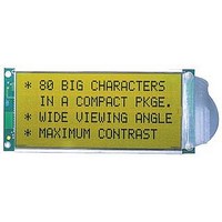
80
Character Count X Line
20 X 4
Character Size
12.1mm
Supply Voltage
5V
Display Mode
Reflective
Display Area Width
144.9mm
Display Area Height
59.5mm


2.2
2.2.1 Instruction Register (IR)
The IR stores instruction codes such as display clear and cursor shift, and address information of the display
data RAM (DD RAM) and character generator RAM (CG RAM). The IR can be written from the MPU, but not
read.
2.2.2 Data Register (DR)
The DR temporarily stores data to be written into or read from the DD RAM or the CG RAM.
2.2.3 Busy Flag
When the Busy Flag is a "1", the module is in an internal operating mode and ignores any additional instructions
(Refer to Read Busy Flag and Address instruction).
2.2.4 Address Counter (AC)
The AC determines the address of the DD RAM or CG RAM in which new data is stored. After writing into (or
reading from) the DD RAM or CG RAM, the AC is incremented or decremented as defined by the
Increment/Decrement bit (Refer to Entry Mode Set instruction).
2.2.5 Display Data RAM (DD RAM)
The DD RAM contains 80 X 8 bits and represents 80 characters. The relationship between the DD RAM
DB4–DB7
DB0–DB3
R/W
RS
E
Industrial Electronic Engineers, Inc.
LCD Controller
4
4
Van Nuys, California
8
7
8
Busy
Flag
Figure 2
8
8
(CG RAM)
Character
Generator
512 Bits
RAM
5
(Parallel Data –Serial Data)
Parallel/Serial Data
Conversion Circuit
7
Counter (AC)
LCD Controller Block Diagram
Address
Display Data
(DD RAM)
(CG ROM)
Character
Generator
80x8 bits
7200 Bits
Scale: NONE
SIZE
RAM
ROM
A
5
8
Timing Generation
7
Circuit
CODE IDENT
05464
NO.
Rev C
40–bit Shift Register
3
16
Sheet 6
S03805–06–0100
Com1–Com16
16
40
Seg1–Seg40
CL1
CL2
M
D
Related parts for 03805-06-0100
Image
Part Number
Description
Manufacturer
Datasheet
Request
R

Part Number:
Description:
92B7890
Manufacturer:
IEE (INDUSTRIAL ELECTRONIC ENGINEERS)
Datasheet:

Part Number:
Description:
Vacuum Fluorescent Display Panel
Manufacturer:
IEE (INDUSTRIAL ELECTRONIC ENGINEERS)

Part Number:
Description:
Vacuum Fluorescent Display Panel
Manufacturer:
IEE (INDUSTRIAL ELECTRONIC ENGINEERS)
Datasheet:

Part Number:
Description:
Vacuum Fluorescent Display Panel
Manufacturer:
IEE (INDUSTRIAL ELECTRONIC ENGINEERS)
Datasheet:

Part Number:
Description:
Vacuum Fluorescent Display Interface System
Manufacturer:
IEE (INDUSTRIAL ELECTRONIC ENGINEERS)
Part Number:
Description:
Vacuum Fluorescent Display Interface System
Manufacturer:
IEE (INDUSTRIAL ELECTRONIC ENGINEERS)

Part Number:
Description:
Vacuum Fluorescent Display Panel
Manufacturer:
IEE (INDUSTRIAL ELECTRONIC ENGINEERS)

Part Number:
Description:
Vacuum Fluorescent Display Panel
Manufacturer:
IEE (INDUSTRIAL ELECTRONIC ENGINEERS)
Part Number:
Description:
Vacuum Fluorescent Display Panel
Manufacturer:
IEE (INDUSTRIAL ELECTRONIC ENGINEERS)
Datasheet:
Part Number:
Description:
Century, 2x40, 5mm, Dot
Manufacturer:
IEE (INDUSTRIAL ELECTRONIC ENGINEERS)
Datasheet:

Part Number:
Description:
Vacuum Fluorescent Display Panel
Manufacturer:
IEE (INDUSTRIAL ELECTRONIC ENGINEERS)

Part Number:
Description:
Vacuum Fluorescent Display Panel
Manufacturer:
IEE (INDUSTRIAL ELECTRONIC ENGINEERS)
Part Number:
Description:
Vacuum Fluorescent Display Panel
Manufacturer:
IEE (INDUSTRIAL ELECTRONIC ENGINEERS)
Part Number:
Description:
Vacuum Fluorescent Display Panel
Manufacturer:
IEE (INDUSTRIAL ELECTRONIC ENGINEERS)
Datasheet:
Part Number:
Description:
12F1025
Manufacturer:
IEE (INDUSTRIAL ELECTRONIC ENGINEERS)
Datasheet: