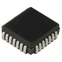
CLC011BCQ National Semiconductor, CLC011BCQ Datasheet - Page 6

CLC011BCQ
Manufacturer Part Number
CLC011BCQ
Description
74C3333
Manufacturer
National Semiconductor
Datasheet
1.CLC011BCQ.pdf
(8 pages)
Specifications of CLC011BCQ
Resolution (bits)
10bit
Input Format
Digital
Output Format
Digital
No. Of Input Channels
2
Supply Voltage Range
4.5V To 5.5V
Operating Temperature Range
0°C To +70°C
Tv / Video Case Style
LCC
Rohs Compliant
No
Available stocks
Company
Part Number
Manufacturer
Quantity
Price
Company:
Part Number:
CLC011BCQ
Manufacturer:
NSC
Quantity:
5 600
Part Number:
CLC011BCQ
Manufacturer:
NS/国半
Quantity:
20 000
Company:
Part Number:
CLC011BCQ/NOPB
Manufacturer:
Texas Instruments
Quantity:
10 000
www.national.com
Input Interfacing—Control Inputs
and a TRS, out of phase with the current PCLK, is received,
output NSP will go high. However, the phase of PCLK will not
be adjusted. NSP will remain high until a TRS, in-phase with
the current PCLK, is received.
FE is normally conditioned in one of three ways.
1. FE tied high. This is the most common mode for FE. In
2. FE tied to NSP. When in this mode, if a TRS that is out
3. FE held low during active video. The automatic fram-
Output Interface—Output Logic
Levels
All outputs of the CLC011 are CMOS compatible. They can
be programmed to provide appropriate output logic levels to
connect to following stages operating from supplies of 3.0V
to 5.5V. Output voltages are set by applying the positive
supply voltage powering the following stage to VDP, which
controls PD0-9, EAV, TRS and NSP, and VCP, which con-
trols PCLK. An example of the CLC011, powered from +5V,
driving a device powered from a 3.3V supply is shown in
Figure 5.
(Continued)
this mode, when a TRS is received, PCLK is aligned to
the new TRS. If a new sync position (NSP) is identified,
the NSP output will go high until the next TRS is re-
ceived.
of phase with the existing PCLK is detected, NSP will go
high, but the phase of PCLK will not be adjusted. If the
next TRS received is in-phase with PCLK, NSP will go
low and the decoder will continue without changing its
state. If the next TRS to arrive is out of phase with PCLK,
then PCLK’s phase is adjusted to meet the new TRS and
NSP is made low. Single erroneous TRS pulses are
ignored in this mode, but if they persist, the decoder will
re-adjust PCLK to properly frame the data.
ing feature using the TRS may be disabled in cases
where non-SMPTE 259M signals are being processed.
In some applications like computer-generated anima-
tion, the serial video data may not adhere to the SMPTE
259M standard and patterns that resemble TSR’s can
occur within the active video line. When such patterns
occur and to prevent the CLC011 from attempting re-
framing, make FE a logic low during the active video
line.
6
The CLC011’s output drivers, shown simplified in Figure 6,
are designed to maintain a constant, controlled slew rate
regardless of load. This design results in lower output
switching noise injection via the supply pins and into other
circuitry. Even so, it is recommended that the CLC011 and
other digital circuitry be separated from analog circuitry and
cable equalizers.
FIGURE 6. Simplified Output Buffer Schematic
FIGURE 5. Typical Output Interface
10008607
10008608


