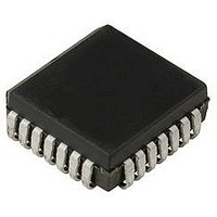
CLC011BCQ National Semiconductor, CLC011BCQ Datasheet - Page 7

CLC011BCQ
Manufacturer Part Number
CLC011BCQ
Description
74C3333
Manufacturer
National Semiconductor
Datasheet
1.CLC011BCQ.pdf
(8 pages)
Specifications of CLC011BCQ
Resolution (bits)
10bit
Input Format
Digital
Output Format
Digital
No. Of Input Channels
2
Supply Voltage Range
4.5V To 5.5V
Operating Temperature Range
0°C To +70°C
Tv / Video Case Style
LCC
Rohs Compliant
No
Available stocks
Company
Part Number
Manufacturer
Quantity
Price
Company:
Part Number:
CLC011BCQ
Manufacturer:
NSC
Quantity:
5 600
Part Number:
CLC011BCQ
Manufacturer:
NS/国半
Quantity:
20 000
Company:
Part Number:
CLC011BCQ/NOPB
Manufacturer:
Texas Instruments
Quantity:
10 000
Output Interface—Control Outputs
PCLK (Parallel Clock): The parallel output or word clock,
PCLK, is synchronous with the parallel data outputs, PD0–9.
The rising edge of PCLK is located at the center of the
parallel data window.
TRS (Timing Reference Signal): The active-low TRS out-
put pulse is four parallel clock periods long. TRS is active
during decoding of both composite and component video
signals.
EAV (End of Active Video): The EAV output is pulsed low
for one cycle of the parallel clock every time an EAV timing
reference is detected during decoding of component video.
The pulse is coincident with the fourth word of the timing
reference (the XYZ word). During reception of composite
video, this output is always asserted high.
NSP (New Sync Position): The active-low NSP output in-
dicates that the most recently received TRS is in a different
position relative to the previous TRS. NSP remains high until
the parallel rate clock is properly aligned with the TRS, then
goes low.
PCB Layout Guidelines
The CLC011 is not as sensitive to PCB layout as some Serial
Digital Video decoders. The following suggestions will help
achieve and maintain optimum system performance.
1. Locate the CLC011 decoder away from equalizers and
2. The trace from the signal input connector to the CLC011
other sensitive circuitry to avoid unwanted crosstalk from
clock and data outputs which may degrade system per-
formance.
must be kept short and should not run parallel to the
data output traces.
7
3. Bypass each power pin with a 0.01 µF to 0.1 µF mono-
4. Power the CLC011 and other clock recovery circuitry
Other PCB layout tips may be found in: “Keeping Analog
Signals Pure in a Hostile Digital World”, Electronic Design,
Special Analog Issue, June 24, 1996, available from National
Semiconductor. Request Literature number 665502-001.
Evaluation Board
Evaluation boards are available for a nominal charge that
demonstrate the basic operation of the SDI/SDV/SDH de-
vices. The evaluation boards can be ordered through Nation-
al’s Distributors. Supplies are limited, please check for cur-
rent availability.
The SD901EVK SMPTE 259M Receiver evaluation kit pro-
vides an operating environment in which the decoder can be
evaluated by system / hardware designers. The evaluation
board has all the needed circuitry and connectors for easy
connection and checkout of the device circuit options as
discussed in the CLC011 datasheet. A schematic, parts list
and pictorial drawing are provided with the board.
From the WWW, the following information may be viewed /
downloaded
www.national.com/appinfo/interface
• Device Datasheet and / or EVK User Manual
• View a picture of the EVK
• View the EVK Schematic
• View the top assembly drawing and BOM
• View the bottom assembly drawing and BOM
lithic ceramic capacitor.
from a separate power supply network from that of other
digital circuitry on the board.
for
most
evaluation
www.national.com
boards:


