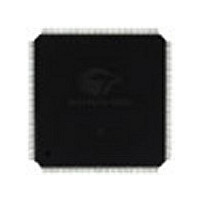
CY7C057V-20AC Cypress Semiconductor Corp, CY7C057V-20AC Datasheet - Page 18

CY7C057V-20AC
Manufacturer Part Number
CY7C057V-20AC
Description
Manufacturer
Cypress Semiconductor Corp
Datasheet
1.CY7C057V-20AC.pdf
(23 pages)
Specifications of CY7C057V-20AC
Density
1.125Mb
Access Time (max)
20ns
Sync/async
Asynchronous
Architecture
Not Required
Clock Freq (max)
Not RequiredMHz
Operating Supply Voltage (typ)
3.3V
Address Bus
15b
Package Type
TQFP
Operating Temp Range
0C to 70C
Number Of Ports
2
Supply Current
340mA
Operating Supply Voltage (min)
3.135V
Operating Supply Voltage (max)
3.465V
Operating Temperature Classification
Commercial
Mounting
Surface Mount
Pin Count
144
Word Size
36b
Number Of Words
32K
Lead Free Status / Rohs Status
Not Compliant
Available stocks
Company
Part Number
Manufacturer
Quantity
Price
Company:
Part Number:
CY7C057V-20AC
Manufacturer:
CY
Quantity:
547
Company:
Part Number:
CY7C057V-20AC
Manufacturer:
CYPRESS
Quantity:
455
Document #: 38-06055 Rev. *B
Right Port Configuration
Right Port Operation
Left Port Operation
When reading a semaphore, data lines 0 through 8 output the
semaphore value. The read value is latched in an output
register to prevent the semaphore from changing state during
a write from the other port. If both ports attempt to access the
semaphore within t
be obtained by one side or the other, but there is no guarantee
which side will control the semaphore.
Notes:
48. BM and SIZE must be configured one clock cycle before operation is guaranteed.
49. In x36 mode WA and BA pins are “Don’t Care.”
50. In x18 mode BA pin is a “Don’t Care.”
51. DQ represents data output of the chip.
Configuration
x36
x18
x18
x9
x9
x9
x9
BM
0
0
1
1
SPS
SPS
SPS
of each other, the semaphore will definitely
of each other, the semaphore will definitely
of each other, the semaphore will definitely
Control Pin
B0
B1
B2
B3
[48, 49, 50]
WA
X
0
1
0
0
1
1
SIZE
0
1
0
1
BA
X
X
X
0
1
0
1
x36 (CE Active SEM Mode)
Bus Match Operation
The right port of the CY7C057V 32Kx36 dual-port SRAM can
be configured in a 36-bit long-word, 18-bit word, or 9-bit byte
format for data I/O. The data lines are divided into four lanes,
each consisting of 9 bits (byte-size data lines).
The Bus Match Select (BM) pin works with Bus Size Select
(SIZE) to select bus width (long-word, word, or byte) for the
right port of the dual-port device. The data sequencing
arrangement is selected using the Word Address (WA) and
Byte Address (BA) input pins. A logic “0” applied to both the
Bus Match Select (BM) pin and to the Bus Size Select (SIZE)
x36
/
Data Accessed
Configuration
x36 (Standard)
DQ
DQ
DQ
16K/32Kx36
x18
DQ
DQ
DQ
CY7C056V
CY7C057V
DQ
Dual Port
x9
18–35
18–26
27–35
0–35
0–17
9–17
0–8
I/O
I/O
I/O
I/O
18–26
27–35
9–17
[51]
0–8
Effect
Byte Control
Byte Control
Byte Control
Byte Control
9
/
9
/
9
/
9
/
BA WA
BM SIZE
I/O Pins Used
I/O Pins Used
I/O
I/O
I/O
CY7C056V
CY7C057V
I/O
I/O
I/O
I/O
I/O
I/O
I/O
I/O
0–35
0–35
0–17
0–8
0–35
0–17
0–17
0–8
0–8
0–8
0–8
x9, x18, x36
Page 18 of 23
/
[+] Feedback


