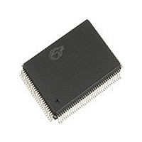
CY7C68013-128AC Cypress Semiconductor Corp, CY7C68013-128AC Datasheet - Page 32

CY7C68013-128AC
Manufacturer Part Number
CY7C68013-128AC
Description
Manufacturer
Cypress Semiconductor Corp
Datasheet
1.CY7C68013-128AC.pdf
(48 pages)
Specifications of CY7C68013-128AC
Cpu Family
FX2LP
Device Core
8051
Device Core Size
8b
Frequency (max)
48MHz
Interface Type
I2C/USB
Program Memory Type
ROMLess
Program Memory Size
Not Required
Total Internal Ram Size
8KB
# I/os (max)
40
Number Of Timers - General Purpose
3
Operating Supply Voltage (typ)
3.3V
Operating Supply Voltage (max)
3.6V
Operating Supply Voltage (min)
3V
Instruction Set Architecture
CISC
Operating Temp Range
0C to 70C
Operating Temperature Classification
Commercial
Mounting
Surface Mount
Pin Count
128
Package Type
TQFP
Lead Free Status / Rohs Status
Not Compliant
Available stocks
Company
Part Number
Manufacturer
Quantity
Price
Company:
Part Number:
CY7C68013-128AC
Manufacturer:
CY
Quantity:
1 000
Part Number:
CY7C68013-128AC
Manufacturer:
CYPRESS/赛普拉斯
Quantity:
20 000
9.4
Table 9-2. Data Memory Write Parameters
When using the AUTPOPTR1 or AUTOPTR2 to address external memory, the address of AUTOPTR1 will only be active while
either RD# or WR# are active. The address of AUTOPTR2 will be active throughout the cycle and meet the above address valid
time for which is based on the stretch value.
Document #: 38-08012 Rev. *F
t
t
t
t
t
t
AV
STBL
STBH
SCSL
ON1
OFF1
Parameter
CLKOUT
CLKOUT
A[15..0]
A[15..0]
D[7..0]
D[7..0]
CS#
CS#
WR#
WR#
Data Memory Write
t
t
Delay from Clock to Valid Address
Clock to WR Pulse LOW
Clock to WR Pulse HIGH
Clock to CS Pulse LOW
Clock to Data Turn-on
Clock to Data Hold Time
AV
AV
t
t
CL
CL
t
SCSL
t
ON1
t
ON1
t
STBL
Figure 9-3. Data Memory Write Timing Diagram
Description
data out
Stretch = 1
data out
t
STBH
Min.
0
0
0
0
0
t
t
OFF1
AV
Max.
10.7
11.2
11.2
13.0
13.1
13.1
Unit
ns
ns
ns
ns
ns
ns
CY7C68013
Page 32 of 48
t
OFF1
Notes


