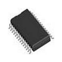
LM9822CCWM National Semiconductor, LM9822CCWM Datasheet

LM9822CCWM
Specifications of LM9822CCWM
Available stocks
Related parts for LM9822CCWM
LM9822CCWM Summary of contents
Page 1
... AGND 11 18 CLMP SEN 12 17 VSMP 16 SDI 13 MCLK 15 14 SDO SCLK T +70°C A Device Marking 1 LM9822CCWM 2 LM9822CCWM 2 - Tape and reel transport media, 1000 parts per reel 1 May 1999 14 Bits 6MHz 5V±5% 3.3V±10% or 5V±5% 375mW NS Package Number M28B M28B www.national.com ...
Page 2
LM9822 Block Diagram V AGND RED OS CDS from CCD OS G GREEN OS CDS from CCD OS B BLUE OS CDS from CCD VClamp SCLK Serial SDI Interface SDO SEN V A Gain Static Coarse Color ...
Page 3
Absolute Maximum Ratings + Positive Supply Voltage ( With Respect GND AGND DGND Voltage On Any Input or Output Pin Input Current at any pin (Note 3) Package Input Current (Note 3) ...
Page 4
Electrical Characteristics (Continued) The following specifications apply for AGND=DGND=0V, V for all other limits MIN MAX A Symbol Parameter Internal Reference Characteristics Mid Reference Output Voltage V REFMID Positive Reference ...
Page 5
... Note 5: Human body model, 100pF capacitor discharged through a 1.5k Note 6: See AN450 “Surface Mounting Methods and Their Effect on Product Reliability” or the section titled “Surface Mount” found in any National Semiconductor Linear Data Book for other methods of soldering surface mount devices. ...
Page 6
Electrical Characteristics Note 9: Typicals are =25° 12MHz, and represent most likely parametric norm MCLK Note 10: Tested limits are guaranteed to National's AOQL (Average Outgoing Quality Level). Note 11: Full channel integral ...
Page 7
Typical Performance Characteristics (Divide by 2, Monochrome Mode, 6 MHz Pixel Rate) Typical 14 Bit DNL 2 1.5 1 LSB 0 4096 8192 Output Code Typical 12 Bit DNL 2 1.5 1 LSB 0.5 0 -0.5 ...
Page 8
Pin Descriptions Analog Power V The two pins are the analog supply pins They should be connected to a voltage source of +5V and bypassed to 0.1µF monolithic capacitor in parallel with a 10µF tantalum capacitor. These two ...
Page 9
Timing Diagrams MCLK VSMP ADC Clock (internal) N-1 Sample Signal Level Sample Reference Level D7 - N-5 DOE (Register 0, Bit Diagram 1: Divide by 6 Color ...
Page 10
Timing Diagrams (Continued MCLK VSMP ADC Clock (internal) N-1 Sample Signal Level Sample Reference Level D7 - N-4 DOE (Register 0, Bit Diagram 4: Divide by 8 Monochrome Mode Sample and Data ...
Page 11
Timing Diagrams (Continued MCLK VSMP Sample Signal Sample Reference D3 -D0 Diagram 7: Programmable Reference Sample Timing OS MCLK VSMP CLMP N-1 Sample Signal N Sample Reference CDSREF = 00 Clamp On ...
Page 12
Timing Diagrams (Continued) t SCLK SCLK SEN t t SSU SH SDI SDO XX MCLK t t VSU VH VSMP t t CSU CH CLMP DDO Diagram 13: MCLK, VSMP ...
Page 13
Table 1: Configuration Register Address Table Address (Binary I/O Mode N/A 0 ...
Page 14
Table 2: Configuration Register Parameters Power-Up Default Register Settings are shown in Bold Italics Parameter (Address) B7 I/O Mode 0 ( DOE 0 D7-D0 are clocked out (change) on the falling edge of MCLK - Recommended setting for ...
Page 15
Table 2: Configuration Register Parameters Power-Up Default Register Settings are shown in Bold Italics Parameter (Address) Red, Green and Blue Offset DAC Settings (1, 2 & Offset Polarity 1 B4(M Offset Value B3 SB (SIGN ...
Page 16
Table 2: Configuration Register Parameters Power-Up Default Register Settings are shown in Bold Italics Parameter (Address (x3) (MSB • • • • • • Typical Gain Values 0 ...
Page 17
Applications Information 1.0 Introduction The LM9822 is a high performance scanner Analog Font End (AFE) for image sensor processing systems designed to work with color CCD and CIS image sensors and provides a full 3 channel sampling, gain ...
Page 18
Applications Information (Continued) 5.0 Offset DAC The Offset DACs remove the DC offsets generated by the sensor and the LM9822’s analog signal chain (see section 5.1, Internal Offsets). The DAC value for each color (registers 1,2 and 3) should be ...
Page 19
Applications Information (Continued) 6.1.1 CDS mode Minimum Clamp Capacitor Calculation: The following equation takes the maximum leakage current into the OS input, the maximum allowable droop, the number of pixels on the sensor, and the pixel conversion rate, f the ...
Page 20
Applications Information (Continued) In this example, a 0.01µF capacitor takes 14 lines after power-up to charge to its final value. On subsequent lines, the only error will be the droop across a single line which should be significantly less than ...
Page 21
Applications Information (Continued) pling point for particular CCD sensors. Diagram 7 shows how the various settings of CDSREF can be used to delay the Reference Sampling point. Care must be taken to avoid setting CDSREF to an inappropriate value when ...
Page 22
... National does not assume any responsibility for use of any circuitry described, no circuit patent licenses are implied and Nati nal reserves the right at any time without notice to change said circuitry and specifications. Order Number LM9822CCWM NS Package Number M28B 2. A critical component is any component of a life support device ...


