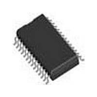
LM9822CCWM National Semiconductor, LM9822CCWM Datasheet - Page 5

LM9822CCWM
Manufacturer Part Number
LM9822CCWM
Description
Manufacturer
National Semiconductor
Datasheet
1.LM9822CCWM.pdf
(22 pages)
Specifications of LM9822CCWM
Operating Temperature (min)
0C
Operating Temperature Classification
Commercial
Operating Temperature (max)
70C
Package Type
SOIC W
Rad Hardened
No
Lead Free Status / Rohs Status
Not Compliant
Available stocks
Company
Part Number
Manufacturer
Quantity
Price
Part Number:
LM9822CCWM
Manufacturer:
NS/国半
Quantity:
20 000
Company:
Part Number:
LM9822CCWMX
Manufacturer:
LATTIC
Quantity:
673
Note 1: Absolute Maximum Ratings indicate limits beyond which damage to the device may occur. Operating Ratings indicate conditions for which the device is functional,
but do not guarantee specific performance limits. For guaranteed specifications and test conditions, see the Electrical Characte ristics. The guaranteed specifications apply
only for the test conditions listed. Some performance characteristics may degrade when the device is not operated under the list ed test conditions.
Note 2: All voltages are measured with respect to GND=AGND=DGND=0V, unless otherwise specified.
Note 3: When the input voltage (V
maximum package input current rating limits the number of pins that can simultaneously safely exceed the power supplies with an input current of 25mA to two.
Note 4: The maximum power dissipation must be derated at elevated temperatures and is dictated by T
able power dissipation at any temperature is P
is 69°C/W for the M28B SOIC package
Note 5: Human body model, 100pF capacitor discharged through a 1.5k
Note 6: See AN450 “Surface Mounting Methods and Their Effect on Product Reliability” or the section titled “Surface Mount” found in any National Semiconductor Linear
Data Book for other methods of soldering surface mount devices.
Note 7: Two diodes clamp the OS analog inputs to
impedance of the sensor, prevents damage to the LM9822 from transients during power-up.
Note 8: To guarantee accuracy, it is required that V
both V
AC Electrical Characteristics
The following specifications apply for AGND=DGND=0V, V
otherwise. Boldface limits apply for
Symbol
t
t
t
f
SDDO
t
MCLK
t
t
t
t
A
SCLK
MCLK
DDO
SEN
SSU
t
VSU
t
CSU
t
CH
SH
VH
and V
D
are operated at 5.0V, they must be powered by the same regulator, with separate power planes or traces and separate bypass capacitors at each supply pin.
Maximum MCLK frequency
MCLK period
MCLK duty cycle
Serial Clock Period
Serial Enable high time
SDI setup time
SDI hold time
SCLK
VSMP setup time
VSMP hold time
CLMP setup time
CLMP hold time
MCLK
edge to new valid data
edge to new valid data
IN
) at any pin exceeds the power supplies (V
Parameter
.
D
= (T
A
A
AGND
=T
J
max - T
and V
J
=T
D
and
MIN
A
be connected to clean, low noise power supplies, with separate bypass capacitors at each supply pin. When
) /
V
OS Input
A
to T
JA
as shown below. This input protection, in combination with the external clamp capacitor and the output
. T
MAX
J
max = 150°C for this device. The typical thermal resistance (
V
V
V
V
A
resistor. Machine model, 200 pF capacitor discharged through a 0
=+5.0V
; all other limits T
D
D
D
D
= 5.0V
= 3.3V
= 5.0V
= 3.3V
IN
AGND
V
<GND or V
A
5
DC
, V
Conditions
D
IN
TO INTERNAL
CIRCUITRY
=+3.0 or +5.0V
>V
A
A
=T
or
V
J
=25°C. (Notes 7& 8)
D ), the current at that pin should be limited to 25mA. The 50m
J
max,
JA
DC
and the ambient temperature, T
, f
MCLK
(Note 9)
Typical
=12MHz, except where noted
8.5
83
19
16
25
JA
) of this part when board mounted
(Note 10)
Limits
12
40
60
20
25
resistor.
1
3
1
3
1
3
1
3
A
. The maximum allow-
www.national.com
t
t
MHz (min)
MCLK
MCLK
ns (max)
ns (max)
ns (max)
(Limits)
ns (min)
ns (min)
ns (min)
ns (min)
ns (min)
ns (min)
ns (min)
%(max)
%(min)
Units
(min)
(min)


