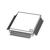
PCF8578H NXP Semiconductors, PCF8578H Datasheet - Page 9

PCF8578H
Manufacturer Part Number
PCF8578H
Description
Manufacturer
NXP Semiconductors
Datasheet
1.PCF8578H.pdf
(48 pages)
Specifications of PCF8578H
Operating Supply Voltage (typ)
3.3/5V
Operating Temperature (min)
-40C
Operating Temperature (max)
85C
Operating Temperature Classification
Industrial
Package Type
LQFP
Pin Count
64
Mounting
Surface Mount
Power Dissipation
400mW
Operating Supply Voltage (min)
2.5V
Operating Supply Voltage (max)
6V
Lead Free Status / Rohs Status
Compliant
Available stocks
Company
Part Number
Manufacturer
Quantity
Price
Part Number:
PCF8578H
Manufacturer:
PHILIPS/飞利浦
Quantity:
20 000
Company:
Part Number:
PCF8578H/1,118
Manufacturer:
NXP Semiconductors
Quantity:
10 000
Company:
Part Number:
PCF8578H/1,157
Manufacturer:
NXP Semiconductors
Quantity:
10 000
Part Number:
PCF8578HT
Manufacturer:
NXP/恩智浦
Quantity:
20 000
Company:
Part Number:
PCF8578HT/1
Manufacturer:
NXP
Quantity:
12 000
Part Number:
PCF8578HT/1
Manufacturer:
NXP/恩智浦
Quantity:
20 000
Company:
Part Number:
PCF8578HT/1,518
Manufacturer:
NXP Semiconductors
Quantity:
10 000
Part Number:
PCF8578HT/1,518
Manufacturer:
NXP/恩智浦
Quantity:
20 000
Company:
Part Number:
PCF8578HT1
Manufacturer:
NXP
Quantity:
6 520
Philips Semiconductors
7.3
The bias levels required to produce maximum contrast
depend on the multiplex rate and the LCD threshold
voltage (V
which the LCD exhibits 10% contrast. Table 2 shows the
optimum voltage bias levels for the PCF8578 as functions
of V
ratios (D) for the different multiplex rates. A practical value
for V
shows the first 4 rows of Table 2 as graphs. Table 3 shows
the relative values of the resistors required in the
configuration of Fig.5 to produce the standard multiplex
rates.
Table 2 Optimum LCD voltages
Table 3 Multiplex rates and resistor values for Fig.5
2003 Apr 14
-------- -
V
-------- -
V
-------- -
V
-------- -
V
V
-------- -
V
--------------------- -
V
-------------------- -
D
V
RESISTORS
V
V
V
V
PARAMETER
LCD row/column driver for
dot matrix graphic displays
op
op
op
op
op
th
off rms
on rms
2
3
4
5
V
op
V
=
op
op
op
(V
R1
R2
R3
--------------------- -
V
V
Multiplexed LCD bias generation
is obtained by equating V
on rms
off rms
op
th
= V
). V
DD
th
is typically defined as the RMS voltage at
V
0.739
0.522
0.478
0.261
0.297
0.430
1.447
3.370
1 : 8
LCD
3
n = 8
n 2
–
), together with the discrimination
MULTIPLEX RATE (n)
R
–
n
MULTIPLEX RATE
R
R
1 : 16
0.800
0.600
0.400
0.200
0.245
0.316
1.291
4.080
off(rms)
with V
1 : 24
0.830
0.661
0.339
0.170
0.214
0.263
1.230
4.680
n = 16, 24, 32
n 3
th
R
R
–
. Figure 4
1 : 32
0.850
0.700
0.300
0.150
0.193
0.230
1.196
5.190
R
9
7.4
At power-on the PCF8578 resets to a defined starting
condition as follows:
1. Display blank
2. 1 : 32 multiplex rate, row mode
3. Start bank, 0 selected
4. Data pointer is set to X, Y address 0, 0
5. Character mode
6. Subaddress counter is set to 0
7. I
Data transfers on the I
following power-on, to allow completion of the reset action.
V
Fig.4
V bias
V op
bias
2
C-bus interface is initialized.
Power-on reset
= V
1.0
0.8
0.6
0.4
0.2
2
0
, V
V
3
bias
, V
4
, V
/V
5
op
. See Table 2.
1:8
as a function of the multiplex rate.
2
C-bus should be avoided for 1 ms
1:16
V 2
V 3
V 4
V 5
Product specification
1:24
multiplex rate
PCF8578
MSA838
1:32


