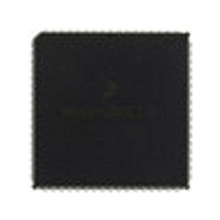
MC68HC711KS2CFN3 Freescale Semiconductor, MC68HC711KS2CFN3 Datasheet - Page 170

MC68HC711KS2CFN3
Manufacturer Part Number
MC68HC711KS2CFN3
Description
Manufacturer
Freescale Semiconductor
Datasheet
1.MC68HC711KS2CFN3.pdf
(290 pages)
Specifications of MC68HC711KS2CFN3
Cpu Family
HC11
Device Core Size
8b
Frequency (max)
4MHz
Interface Type
SCI/SPI
Program Memory Type
ROM
Program Memory Size
32KB
Total Internal Ram Size
1KB
# I/os (max)
51
Number Of Timers - General Purpose
8
Operating Supply Voltage (typ)
5V
Operating Supply Voltage (max)
5.5V
Operating Supply Voltage (min)
4.5V
On-chip Adc
8-chx8-bit
Instruction Set Architecture
CISC
Operating Temp Range
-40C to 85C
Operating Temperature Classification
Industrial
Mounting
Surface Mount
Pin Count
68
Package Type
PLCC
Lead Free Status / Rohs Status
Not Compliant
Available stocks
Company
Part Number
Manufacturer
Quantity
Price
Company:
Part Number:
MC68HC711KS2CFN3
Manufacturer:
NSC
Quantity:
1 001
- Current page: 170 of 290
- Download datasheet (4Mb)
Serial Peripheral Interface (SPI)
8.4 SPI Signal Descriptions
8.4.1 Master In Slave Out (MISO)
8.4.2 Master Out Slave In (MOSI)
8.4.3 Serial Clock (SCK)
Technical Data
170
The four basic SPI signals (MISO, MOSI, SCK, and SS) are discussed
for both the master and slave modes in the following paragraphs.
Every SPI output line must have its corresponding port D data direction
register (DDRD) bit set. If this bit is clear, the line is disconnected from
the SPI logic and becomes a general-purpose input line. SPI input lines
are not affected by the data direction register.
The MISO is one of two unidirectional serial data lines in the SPI. It
functions as an input in a master device and as an output in a slave
device. The MISO line of a slave device is placed in the high-impedance
state if the slave is not selected.
This unidirectional serial data line is an output in a master device and an
input in a slave device.
The serial clock (SCK) synchronizes data movement both in and out of
all devices. Master and slave devices exchange a byte of information
simultaneously during a sequence of eight clock cycles. SCK is
generated by the master device so its SCK pin functions as an output.
Slave devices receive this signal through their SCK pins, which are
configured as inputs.
The SPI clock rate select bits in the master device determine the SCK
clock rate. These bits are SPR[1:0] in the serial peripheral control
register (SPCR) and SPR2 in the system configuration options 2 register
(OPT2). These bits have no effect in a slave device.
Freescale Semiconductor, Inc.
For More Information On This Product,
Serial Peripheral Interface (SPI)
Go to: www.freescale.com
M68HC11K Family
MOTOROLA
Related parts for MC68HC711KS2CFN3
Image
Part Number
Description
Manufacturer
Datasheet
Request
R

Part Number:
Description:
APPENDIX A ELECTRICAL CHARACTERISTICS
Manufacturer:
FREESCALE [Freescale Semiconductor, Inc]
Datasheet:
Part Number:
Description:
Manufacturer:
Freescale Semiconductor, Inc
Datasheet:
Part Number:
Description:
Manufacturer:
Freescale Semiconductor, Inc
Datasheet:
Part Number:
Description:
Manufacturer:
Freescale Semiconductor, Inc
Datasheet:
Part Number:
Description:
Manufacturer:
Freescale Semiconductor, Inc
Datasheet:
Part Number:
Description:
Manufacturer:
Freescale Semiconductor, Inc
Datasheet:
Part Number:
Description:
Manufacturer:
Freescale Semiconductor, Inc
Datasheet:
Part Number:
Description:
Manufacturer:
Freescale Semiconductor, Inc
Datasheet:
Part Number:
Description:
Manufacturer:
Freescale Semiconductor, Inc
Datasheet:
Part Number:
Description:
Manufacturer:
Freescale Semiconductor, Inc
Datasheet:
Part Number:
Description:
Manufacturer:
Freescale Semiconductor, Inc
Datasheet:
Part Number:
Description:
Manufacturer:
Freescale Semiconductor, Inc
Datasheet:
Part Number:
Description:
Manufacturer:
Freescale Semiconductor, Inc
Datasheet:
Part Number:
Description:
Manufacturer:
Freescale Semiconductor, Inc
Datasheet:
Part Number:
Description:
Manufacturer:
Freescale Semiconductor, Inc
Datasheet:


