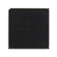
MC68HC711KS2CFN3 Freescale Semiconductor, MC68HC711KS2CFN3 Datasheet - Page 213

MC68HC711KS2CFN3
Manufacturer Part Number
MC68HC711KS2CFN3
Description
Manufacturer
Freescale Semiconductor
Datasheet
1.MC68HC711KS2CFN3.pdf
(290 pages)
Specifications of MC68HC711KS2CFN3
Cpu Family
HC11
Device Core Size
8b
Frequency (max)
4MHz
Interface Type
SCI/SPI
Program Memory Type
ROM
Program Memory Size
32KB
Total Internal Ram Size
1KB
# I/os (max)
51
Number Of Timers - General Purpose
8
Operating Supply Voltage (typ)
5V
Operating Supply Voltage (max)
5.5V
Operating Supply Voltage (min)
4.5V
On-chip Adc
8-chx8-bit
Instruction Set Architecture
CISC
Operating Temp Range
-40C to 85C
Operating Temperature Classification
Industrial
Mounting
Surface Mount
Pin Count
68
Package Type
PLCC
Lead Free Status / Rohs Status
Not Compliant
Available stocks
Company
Part Number
Manufacturer
Quantity
Price
Company:
Part Number:
MC68HC711KS2CFN3
Manufacturer:
NSC
Quantity:
1 001
- Current page: 213 of 290
- Download datasheet (4Mb)
9.9.2 Pulse-Width Modulation Control Registers
9.9.2.1 Pulse-Width Modulation Timer Clock Select Register
M68HC11K Family
MOTOROLA
Address: $0060
Figure 9-31. Pulse-Width Modulation Timer Clock Select (PWCLK)
The three clocks are derived from the E clock by writing to registers
which determine their scaling factors. The clock A frequency is equal to
E divided by 1, 2, 4, or 8, depending on which bits (PCKA[2:1]) in the
PWCLK register are set. The clock B frequency is equal to the E clock
divided by a power of two determined by bits PCKB[3:1] in the PWCLK
register. Clock S is derived by dividing clock A by the integer (1 to 256)
stored in the PWSCAL register, then by two.
Two channels can be concatenated by setting the appropriate bit
(CON34 or CON12) in the PWCLK register. In this mode, the clock
source is determined by the low-order channel, which is channel two in
CON12 and channel four in CON34. The output is also placed on the pin
associated with the low-order channels, so when two channels are
concatenated the pin associated with the high-order channel (PH0
and/or PH2) can be used for GPIO. A read of the high-order byte causes
the low-order byte to be latched for one cycle to guarantee that
double-byte reads are accurate. A write to the low-order byte of the
counter causes reset of the entire counter. A write to the high-order byte
of the counter has no effect.
The PWM control registers are described here.
Reset:
Read:
Write:
Freescale Semiconductor, Inc.
For More Information On This Product,
CON34
Bit 7
0
Go to: www.freescale.com
CON12
Timing System
6
0
PCKA2
5
0
PCKA1
4
0
3
0
0
Pulse-Width Modulator (PWM)
PCKB3
2
0
PCKB2
1
0
Timing System
Technical Data
PCKB1
Bit 0
0
213
Related parts for MC68HC711KS2CFN3
Image
Part Number
Description
Manufacturer
Datasheet
Request
R

Part Number:
Description:
APPENDIX A ELECTRICAL CHARACTERISTICS
Manufacturer:
FREESCALE [Freescale Semiconductor, Inc]
Datasheet:
Part Number:
Description:
Manufacturer:
Freescale Semiconductor, Inc
Datasheet:
Part Number:
Description:
Manufacturer:
Freescale Semiconductor, Inc
Datasheet:
Part Number:
Description:
Manufacturer:
Freescale Semiconductor, Inc
Datasheet:
Part Number:
Description:
Manufacturer:
Freescale Semiconductor, Inc
Datasheet:
Part Number:
Description:
Manufacturer:
Freescale Semiconductor, Inc
Datasheet:
Part Number:
Description:
Manufacturer:
Freescale Semiconductor, Inc
Datasheet:
Part Number:
Description:
Manufacturer:
Freescale Semiconductor, Inc
Datasheet:
Part Number:
Description:
Manufacturer:
Freescale Semiconductor, Inc
Datasheet:
Part Number:
Description:
Manufacturer:
Freescale Semiconductor, Inc
Datasheet:
Part Number:
Description:
Manufacturer:
Freescale Semiconductor, Inc
Datasheet:
Part Number:
Description:
Manufacturer:
Freescale Semiconductor, Inc
Datasheet:
Part Number:
Description:
Manufacturer:
Freescale Semiconductor, Inc
Datasheet:
Part Number:
Description:
Manufacturer:
Freescale Semiconductor, Inc
Datasheet:
Part Number:
Description:
Manufacturer:
Freescale Semiconductor, Inc
Datasheet:


