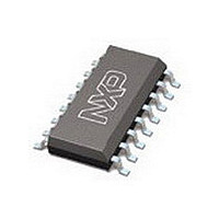
SA5219D NXP Semiconductors, SA5219D Datasheet - Page 4

SA5219D
Manufacturer Part Number
SA5219D
Description
Manufacturer
NXP Semiconductors
Datasheet
1.SA5219D.pdf
(18 pages)
Specifications of SA5219D
Number Of Channels
1
Supply Current
50@5VmA
Operating Supply Voltage (min)
4.5V
Operating Supply Voltage (typ)
5V
Operating Supply Voltage (max)
7V
Power Dissipation
1.1W
Package Type
SO
Mounting
Surface Mount
Pin Count
16
Noise Figure (typ)
9.3@50MHzdB
Operating Temp Range
-40C to 85C
Operating Temperature Classification
Industrial
Lead Free Status / Rohs Status
Compliant
Available stocks
Company
Part Number
Manufacturer
Quantity
Price
Part Number:
SA5219D
Manufacturer:
NXP/恩智浦
Quantity:
20 000
1. With R
Philips Semiconductors
AC ELECTRICAL CHARACTERISTICS
T
NOTE:
SA5219 APPLICATIONS
The SA5219 is a wideband variable gain amplifier (VGA) circuit
which finds many applications in the RF, IF and video signal
processing areas. This application note describes the operation of
the circuit and several applications of the VGA. The simplified
equivalent schematic of the VGA is shown in Figure 2. Transistors
Q1-Q6 form the wideband Gilbert multiplier input stage which is
biased by current source I1. The top differential pairs are biased
from a buffered and level-shifted signal derived from the V
and the RF input appears at the lower differential pair. The circuit
topology and layout offer low input noise and wide bandwidth. The
second stage is a differential transimpedance stage with current
feedback which maintains the wide bandwidth of the input stage.
The output stage is a pair of emitter followers with 50 output
impedance. There is also an on-chip bandgap reference with
buffered output at 1.3V, which can be used to derive the gain control
voltage.
Both the inputs and outputs should be capacitor coupled or DC
isolated from the signal sources and loads. Furthermore, the two
inputs should be DC isolated from each other and the two outputs
should likewise be DC isolated from each other. The SA5219 was
designed to provide optimum performance from a 5V power source.
However, there is some range around this value (4.5 - 7V) that can
be used.
The input impedance is about 1k . The main advantage to a
differential input configuration is to provide the balun function.
1997 Nov 07
A
SYMBOL
SYMBOL
Wideband variable gain amplifier
BW
IP3
= 25
V
V
V
G/ V
P
occurs at input for single-ended gain < 6dB and at output for single-ended gain > 6dB.
V
P
IP3
S12
BW
OMAX
OMAX
IN-EQ
G/ T
O-1dB
C
GF
IMAX
NF
I-1dB
G
AGC
OUT
IN
AB
o
IN
C, V
CC
L
> 1k , overload occurs at input for single-ended gain < 13dB and at output for single-ended gain > 13dB. With R
CC1
-3dB bandwidth
Gain flatness
Maximum input voltage swing (single-ended) for
linear operation
Maximum output voltage swing (single-ended)
Noise figure (unmatched configuration)
Equivalent input noise voltage spectral density
Reverse isolation
Gain supply sensitivity (single-ended)
Gain temperature sensitivity
Input capacitance (single-ended)
-3dB bandwidth of gain control function
1dB gain compression point at output
1dB gain compression point at input
Third-order intercept point at output
Third-order intercept point at input
Gain match output A to output B
for linear operation
= V
CC2
= +5.0V, V
PARAMETER
PARAMETER
1
AGC
1
= 1.0V, unless otherwise specified.
AGC
input
f = 100MHz, V
R
TEST CONDITIONS
TEST CONDITIONS
f = 100MHz, V
f = 100MHz, V
f = 100MHz, V
S
= 50 , f = 50MHz
DC - 500MHz
4
f = 100MHz
f = 100MHz
f = 100MHz
R
R
R
L
L
L
=0.1V
>0.5V
<0.5V
Otherwise, there is an advantage to common mode rejection, a
specification that is not normally important to RF designs. The
source impedance can be chosen for two different performance
characteristics: Gain, or noise performance. Gain optimization will
be realized if the input impedance is matched to about 1k . A 4:1
balun will provide such a broadband match from a 50 source.
Noise performance will be optimized if the input impedance is
matched to about 200 . A 2:1 balun will provide such a broadband
match from a 50 source. The minimum noise figure can then be
expected to be about 7dB. Maximum gain will be about 23dB for a
single-ended output. If the differential output is used and properly
matched, nearly 30dB can be realized. With gain optimization, the
noise figure will degrade to about 8dB. With no matching unit at the
input, a 9dB noise figure can be expected from a 50 source. If the
source is terminated, the noise figure will increase to about 15dB.
All these noise figures will occur at maximum gain.
The SA5219 has an excellent noise figure vs gain relationship. With
any VGA circuit, the noise performance will degrade with decreasing
gain.
each 2dB gain reduction. With the input matched for optimum gain,
the 8dB noise figure at 23dB gain will degrade to about a 20dB
noise figure at 0dB gain.
The SA5219 also displays excellent linearity between voltage gain
and control voltage. Indeed, the relationship is of sufficient linearity
that high fidelity AM modulation is possible using the SA5219. A
= 50
= 1k
= 50
AGC
The 5219 has about a 1.2dB noise figure degradation for
AGC
AGC
AGC
= 1V
MIN
LIMITS
0.013
TYP
+0.4
+13
700
200
400
1.9
9.3
2.5
-60
0.3
-10
0.1
20
+5
-3
2
MAX
Product specification
L
= 50 , overload
SA5219
nV/ Hz
mV
mV
dB/ C
UNIT
UNIT
dB/V
MHz
V
MHz
dBm
dBm
dBm
dBm
dB
dB
dB
pF
dB
P-P
P-P
P-P


