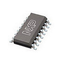
SA5219D NXP Semiconductors, SA5219D Datasheet - Page 5

SA5219D
Manufacturer Part Number
SA5219D
Description
Manufacturer
NXP Semiconductors
Datasheet
1.SA5219D.pdf
(18 pages)
Specifications of SA5219D
Number Of Channels
1
Supply Current
50@5VmA
Operating Supply Voltage (min)
4.5V
Operating Supply Voltage (typ)
5V
Operating Supply Voltage (max)
7V
Power Dissipation
1.1W
Package Type
SO
Mounting
Surface Mount
Pin Count
16
Noise Figure (typ)
9.3@50MHzdB
Operating Temp Range
-40C to 85C
Operating Temperature Classification
Industrial
Lead Free Status / Rohs Status
Compliant
Available stocks
Company
Part Number
Manufacturer
Quantity
Price
Part Number:
SA5219D
Manufacturer:
NXP/恩智浦
Quantity:
20 000
Philips Semiconductors
maximum control voltage frequency of about 20MHz permits video
baseband sources for AM.
A stabilized bandgap reference voltage is made available on the
SA5219 (Pin 7). For fixed gain applications this voltage can be
resistor divided, and then fed to the gain control terminal (Pin 8).
Using the bandgap voltage reference for gain control produces very
stable gain characteristics over wide temperature ranges. The gain
setting resistors are not part of the RF signal path, and thus stray
capacitance here is not important.
The wide bandwidth and excellent gain control linearity make the
SA5219 VGA ideally suited for the automatic gain control (AGC)
function in RF and IF processing in cellular radio base stations,
Direct Broadcast Satellite (DBS) decoders, cable TV systems, fiber
optic receivers for wideband data and video, and other radio
communication applications. A typical AGC configuration using the
SA5219 is shown in Figure 3. Three SA5219s are cascaded with
appropriate AC coupling capacitors. The output of the final stage
drives the full-wave rectifier composed of two UHF Schottky diodes
1997 Nov 07
Wideband variable gain amplifier
V
0–1V
AGC
+
–
RF/IF
INPUT
V
CC
IN
IN
B
A
5219
Q
R
1
1
Q
5
Figure 3. AGC Configuration Using Cascaded SA5219s
Q
2
I
1
Figure 2. Equivalent Schematic of VGA
Q
5219
3
Q
6
Q
4
R
2
R6
5
5230
C4
R4
BAT17 as shown. The diodes are biased by R1 and R2 to V
that a quiescent current of about 2mA in each leg is achieved. An
SA5230 low voltage op amp is used as an integrator which drives
the V
frequency ripple from the full-wave rectified signal. A voltage
divider is used to generate the reference for the non-inverting input
of the op amp at about 1.7V. Keeping D3 the same type as D1 and
D2 will provide a first order compensation for the change in Schottky
voltage over the operating temperature range and improve the AGC
performance. R6 is a variable resistor for adjustments to the op
amp reference voltage. In low cost and large volume applications
this could be replaced with a fixed resistor, which would result in a
slight loss of the AGC dynamic range. Cascading three SA5219s
will give a dynamic range in excess of 60dB.
The SA5219 is a very user-friendly part and will not oscillate in most
applications. However, in an application such as with gains in
excess of 60dB and bandwidth beyond 100MHz, good PC board
layout with proper supply decoupling is strongly recommended.
–
+
5219
AGC
A1
R
R
pin on all three SA5219s. R3 and C3 filter the high
4
3
D1
L1
R5
R3
REFERENCE
R1
BANDGAP
BAT 17
BAT 17
D3
C3
L2
I
R2
2
V
CC
Q
D2
8
50
V
V
BG
CC
OUT
B
AGC
OUTPUT
SR00275
I
3
Q
7
Product specification
50
SA5219
SR00274
OUT
A
CC
such


