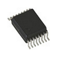
TDA5102NT Infineon Technologies, TDA5102NT Datasheet - Page 13

TDA5102NT
Manufacturer Part Number
TDA5102NT
Description
Manufacturer
Infineon Technologies
Datasheet
1.TDA5102NT.pdf
(35 pages)
Specifications of TDA5102NT
Operating Temperature (max)
85C
Operating Temperature Classification
Commercial
Product Depth (mm)
4.4mm
Operating Supply Voltage (min)
2.1V
Operating Supply Voltage (typ)
2.5/3.3V
Lead Free Status / Rohs Status
Not Compliant
Wireless Components
12
13
14
15
16
FSKGND
PAGND
PAOUT
CSEL
FSEL
15
16
V
V
S
S
90 kΩ
60 kΩ
+1.2 V
+1.2 V
30 kΩ
60 kΩ
V
S
14
13
30 µA
5 µA
3 - 6
+1.1 V
+0.8 V
Ground connection for FSK modulation out-
put FSKOUT.
Ground connection of the power amplifier.
The RF ground return path of the power
amplifier output PAOUT (pin 14) has to be
concentrated to this pin.
RF output pin of the transmitter.
A DC path to the positive supply VS has to
be supplied by the antenna matching net-
work.
This pin has to be left open to select the
915 MHz transmitter frequency range.
A logic low (FSEL < 0.5 V) applied to this pin
sets the transmitter to the 457 MHz fre-
quency range.
A logic high (FSEL open) applied to this pin
sets the transmitter to the 915 MHz fre-
quency range.
This pin is used to select the desired refer-
ence frequency.
A logic low (CSEL < 0.2 V) applied to this pin
sets the internal frequency divider to accept
a reference frequency of 7.15 MHz.
A logic high (CSEL open) applied to this pin
sets the internal frequency divider to accept
a reference frequency of 14.3 MHz.
Specification, October 2001
Functional Description
TDA 5102


